Semiconductor device with protection circuit
A technology for protecting circuits and semiconductors, applied in semiconductor devices, electric solid state devices, semiconductor/solid state device components, etc., can solve problems such as high voltage, non-terminal breakdown, gate insulating film breakdown, etc. Effect
- Summary
- Abstract
- Description
- Claims
- Application Information
AI Technical Summary
Problems solved by technology
Method used
Image

Examples
Embodiment Construction
[0032] A preferred embodiment of the present invention will be described with reference to the accompanying drawings.
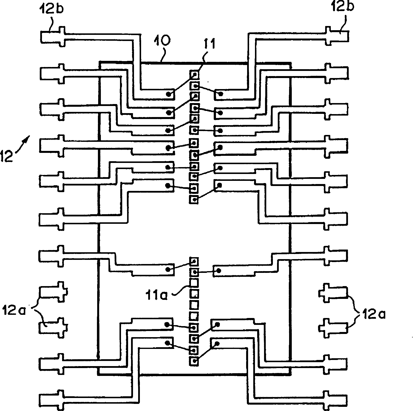
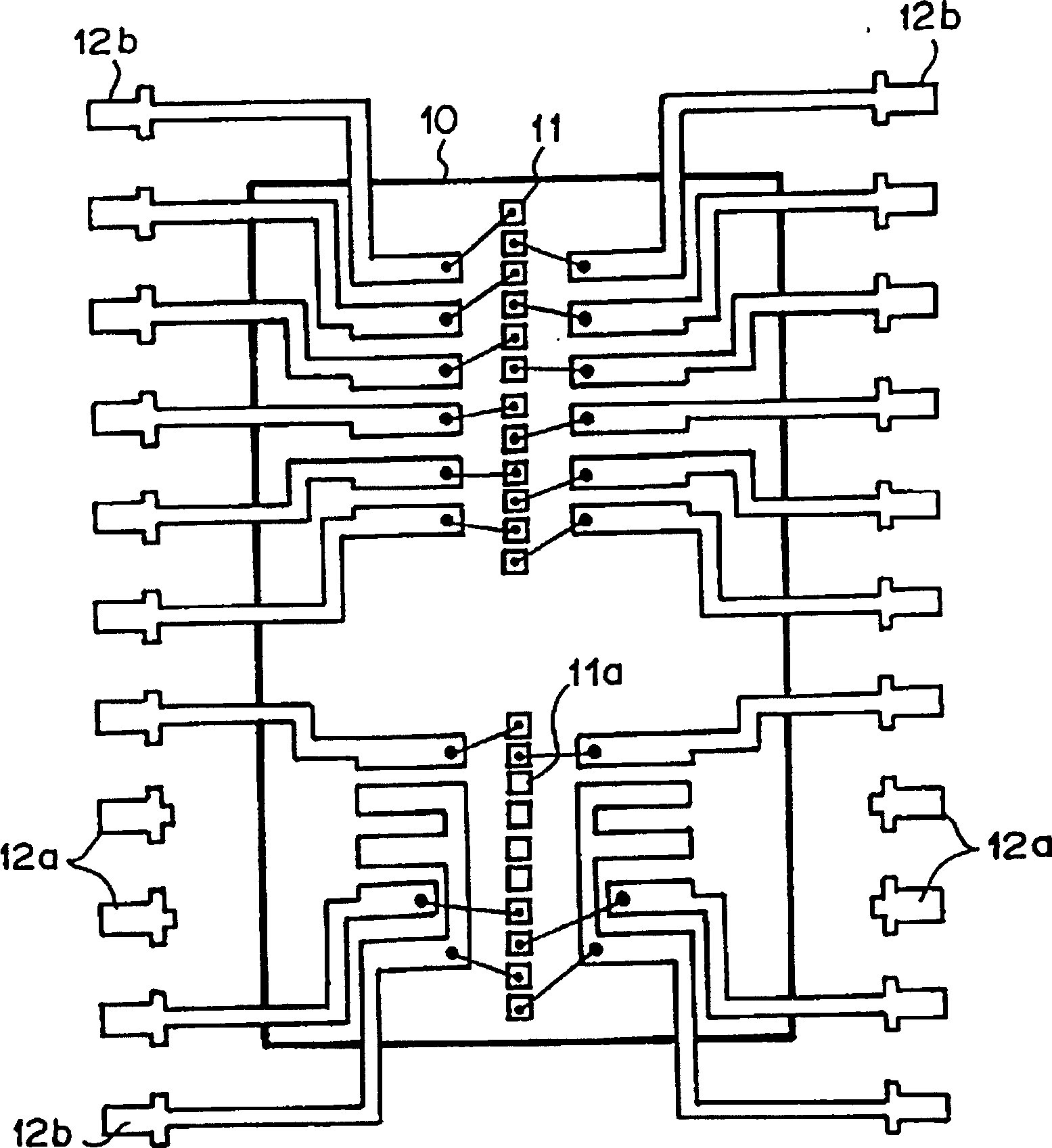
[0033] Such as figure 1 The LOC semiconductor device of an embodiment of the present invention shown in includes a semiconductor chip 10, and a plurality of pads (22 of which are shown) 11 on the semiconductor chip 10, a plurality of terminals or wires 12 ( 22 of them are shown). The four pads 11a among the pads 11 arranged on the semiconductor chip 10 are optional pads which are not electrically connected to any lead 12, and the four leads 12a among the plurality of leads 12 are not connected to any pad 11. connected. The other eighteen leads are terminals 12b.
[0034] Such as figure 1 As shown in , the non-terminal 12a is not electrically connected to any alternative pad 11a, while the terminal 12b is electrically connected to the pad 11. Non-connection terminals (leads) 12a and connection terminals 12b are sealed together with the semiconductor chip ...
PUM
 Abstract
Description
Claims
Application Information
 - R&D Engineer
- R&D Manager
- IP Professional
- Industry Leading Data Capabilities
- Powerful AI technology
- Patent DNA Extraction
Browse by: Latest US Patents, China's latest patents, Technical Efficacy Thesaurus, Application Domain, Technology Topic.
© 2024 PatSnap. All rights reserved.Legal|Privacy policy|Modern Slavery Act Transparency Statement|Sitemap