Packaging structure of LED and packaging method thereof

A technology of light-emitting diodes and packaging structures, which is applied in the direction of electrical components, circuits, semiconductor devices, etc., and can solve problems such as offset, packaging size and difficult control of spectrum

Inactive Publication Date: 2007-05-23
TOPSON OPTOELECTRONICS SEMI CONDUCTOR
View PDF2 Cites 0 Cited by
  • Summary
  • Abstract
  • Description
  • Claims
  • Application Information

AI Technical Summary

Problems solved by technology

[0007] Another object of the present invention is to provide a packaging method for light-emitting diodes, which is to use the mold method to package LED modules to shape LED components with fixed dimensions, and then provide white LEDs with stable spectral ranges to solve the problem of known packaging dimensions. It is difficult to control the problem of spectral shift, so it has the effect of making the light color of white light LED accurate.

Method used


Image

  • Packaging structure of LED and packaging method thereof
  • Packaging structure of LED and packaging method thereof
  • Packaging structure of LED and packaging method thereof

Examples


Embodiment Construction

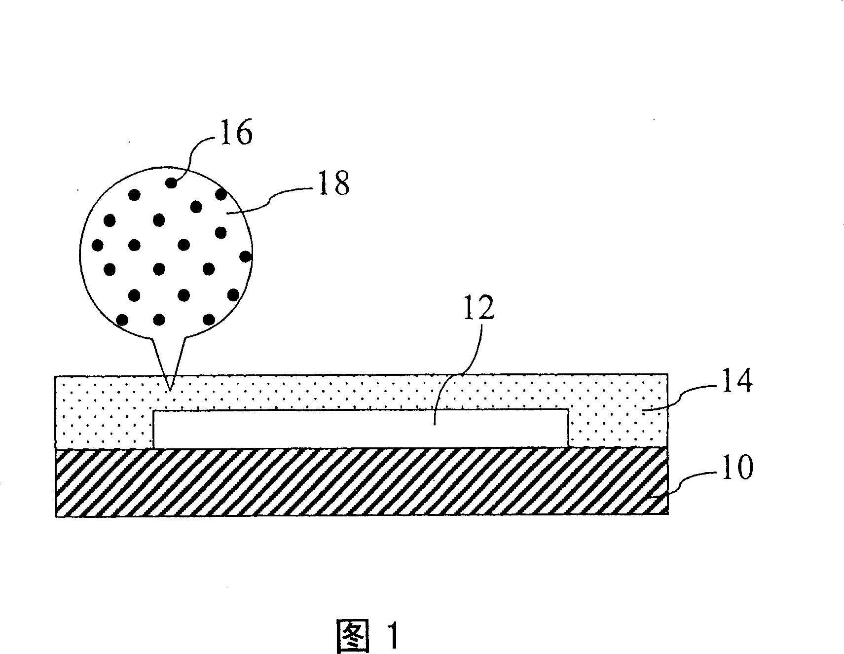
[0034] The light-emitting diode (LED) module packaging technology of the present invention uses liquid phosphor-containing gel as the module packaging material, and uses a mold method and is based on the principle of liquid-saturated solid precipitation and solidification to produce an LED packaging structure.

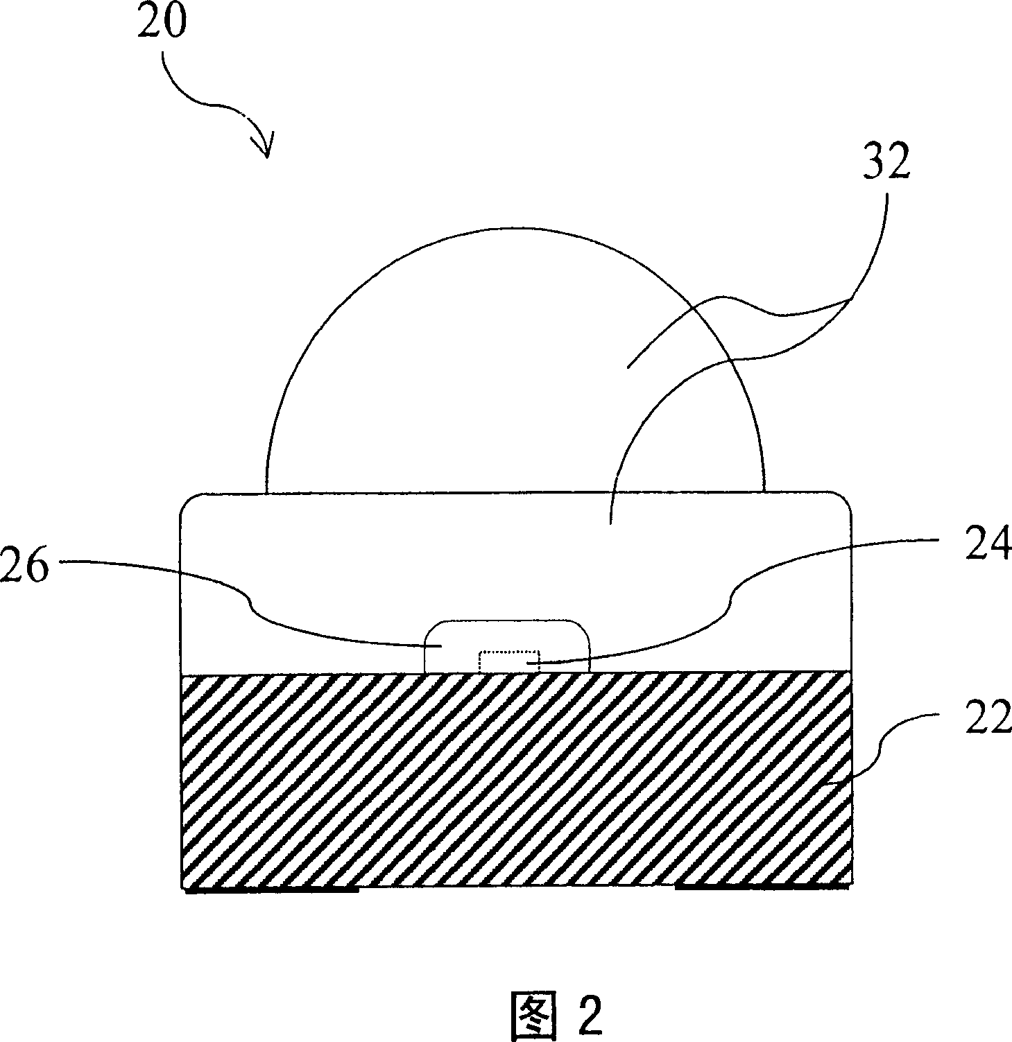
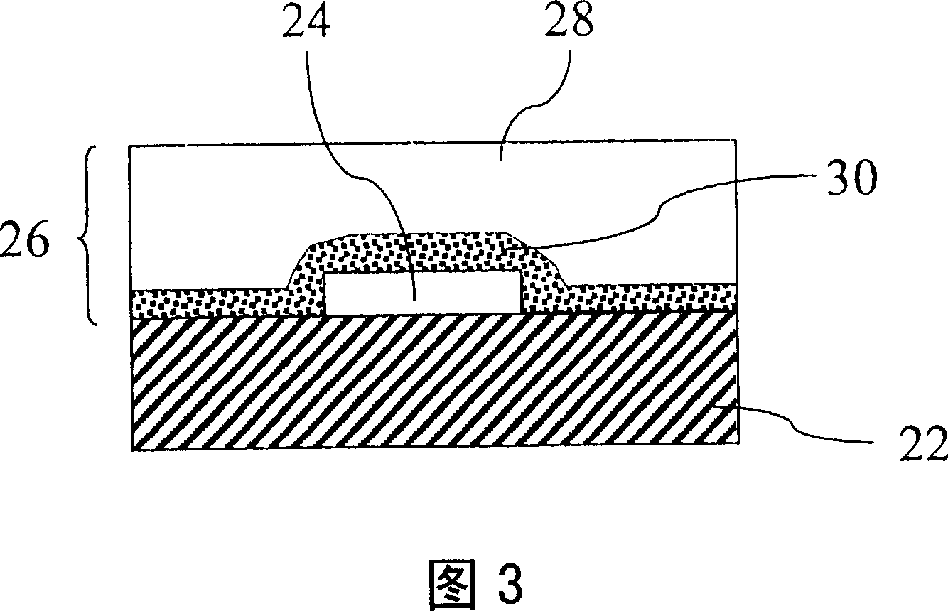
[0035] Please refer to FIG. 2, which is a cross-sectional view of the light-emitting diode packaging structure of the present invention. An LED packaging component 20 includes a substrate 22, which is usually a printed circuit board (PCB) or a metal frame. A light-emitting diode (LED) unit is mounted on the substrate 22, which is an LED die 24, and a phosphorescent medium layer 26 covers the substrate 22 to cover the LED die 24, and an external encapsulant 32 is coated Outside the phosphorescent medium layer 26; wherein the phosphorescent medium layer 26, as shown in FIG. 3, contains an encapsulation gel 28, and a phosphor precipitation layer 30 is deposited on the bottom ...


PUM


Abstract

The invention provides a packaging structure and the method for a kind of illuminant diode, it uses the liquid phosphorus light agent glue as material, and uses the model-casting and forming method to carry on package, in the packaging process, the glue solvent is saturate and the solid phosphorus light agent is deposited, thus, a phosphorus light media layer covers the illuminant diode, the phosphorus media layer contains a packaging glue and a phosphorus light agent layer, the phosphorus light agent are coated on the illuminant diode. The invention can realize the low color leakage rate effect, at the same time, the size is standardized, the white light spectrum is stable, and it can save the materials.

Description

Technical field [0001] The invention relates to a light emitting diode packaging technology, in particular to a white light emitting diode packaging structure and packaging method. Background technique [0002] Generally, the packaging of light-emitting diodes (LEDs) is carried out by transfer molding or liquid dispensing packaging. Transfer injection molding is currently the most commonly used process, which is to place the printed circuit board (PCB) or metal frame (metal frame) with LED chips and wires attached to the casting hole of the transfer molding mold. In the cavity, the preheated and softened solid granular epoxy resin is pressure-injected into the casting hole of the transfer mold by an extrusion rod (ram), and the epoxy resin material is heated to produce a hardening reaction, which completes the module encapsulation process. Then it is cut into multiple LED package components. However, for small-sized LED products, due to the long raw material conveying tank of the...

Claims


Application Information

Patent Timeline
Patent Type & Authority Patents(China)
IPC IPC(8): H01L33/00
Inventor 林荣淦
Owner TOPSON OPTOELECTRONICS SEMI CONDUCTOR
Why Eureka
Try Eureka