Packaging structure of LED and packaging method thereof

A technology of light-emitting diodes and packaging structures, which is applied to electrical components, circuits, semiconductor devices, etc., and can solve problems such as difficult control of spectrum and offset

Inactive Publication Date: 2004-11-17
TOPSON OPTOELECTRONICS SEMI CONDUCTOR
View PDF0 Cites 19 Cited by
  • Summary
  • Abstract
  • Description
  • Claims
  • Application Information

AI Technical Summary

Problems solved by technology

[0007] Another object of the present invention is to provide a method for packaging light-emitting diodes, which uses a molding method to mold LEDs to form LED elements with fixed dimensions, thereby providing white LEDs with...

Method used


Image

  • Packaging structure of LED and packaging method thereof
  • Packaging structure of LED and packaging method thereof
  • Packaging structure of LED and packaging method thereof

Examples


Embodiment Construction

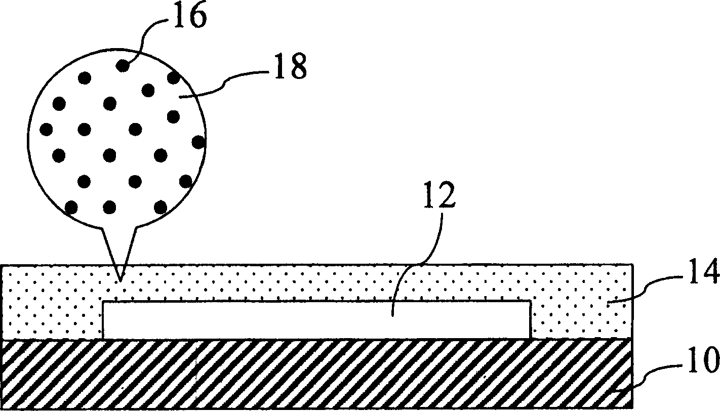
[0034] The light-emitting diode (LED) molding technology of the present invention uses liquid colloid containing phosphor (Phosphor) as the molding raw material, utilizes the casting method and is based on the solidification principle of the liquid-saturated solid sink, and manufactures the LED packaging structure.

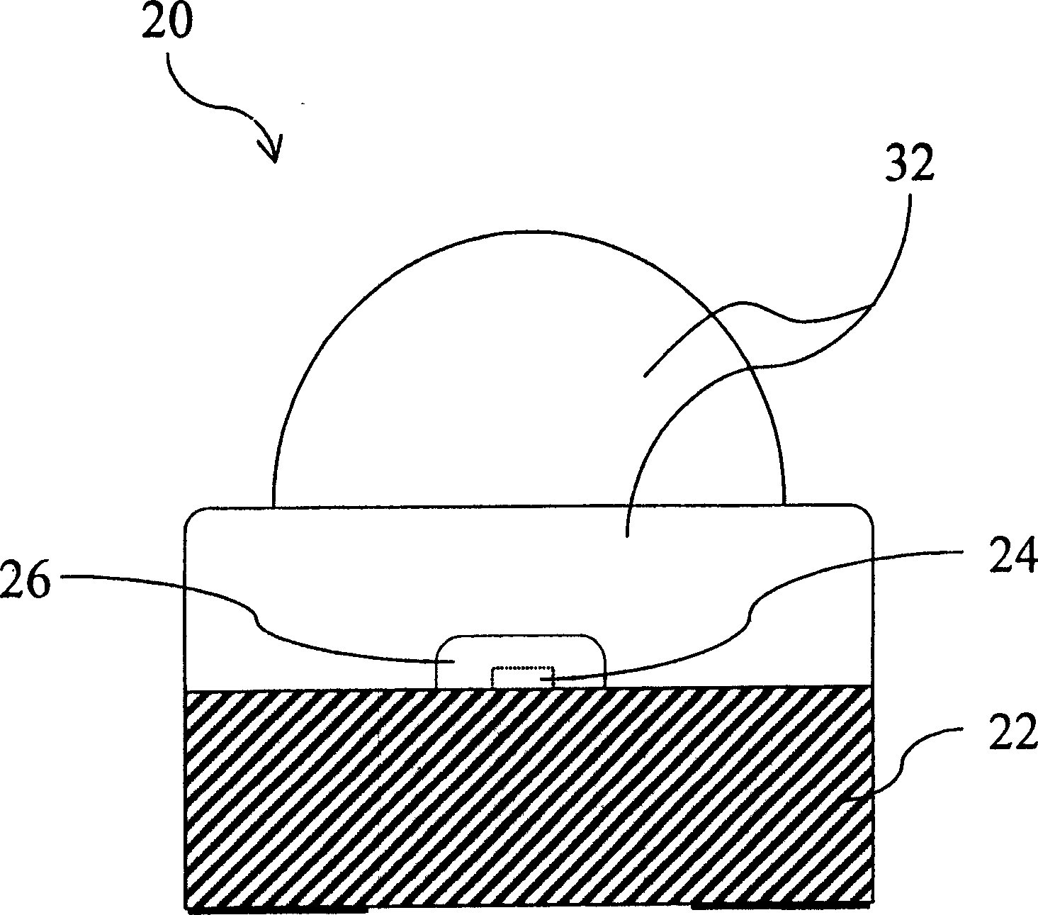
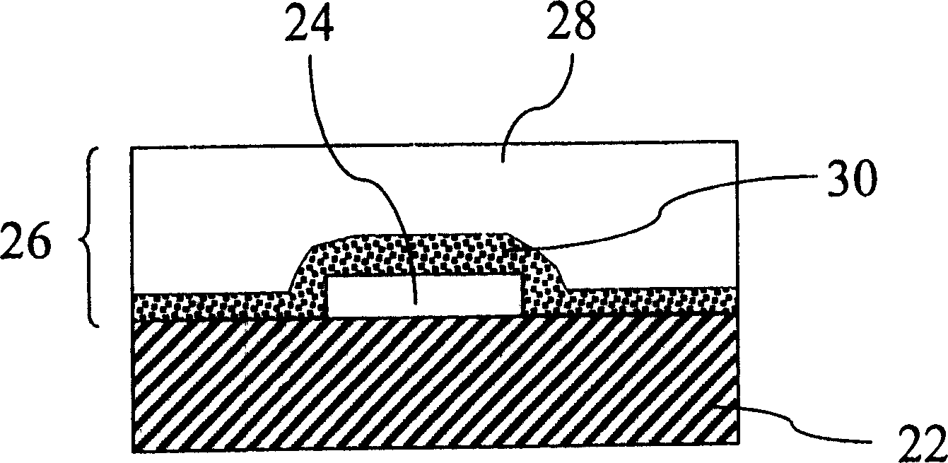
[0035] Please refer to figure 2 As shown, it is a cross-sectional view of the LED packaging structure of the present invention. An LED packaging component 20 includes a substrate 22, which is usually a printed circuit board (PCB) or a metal frame (metal frame). A light-emitting diode (LED) unit is installed on it, which is an LED crystal grain 24, and a phosphorescent medium layer 26 is coated on the substrate 22 to cover the LED crystal grain 24, and an external encapsulant 32 is coated on the phosphorescent outside the dielectric layer 26; wherein the phosphorescent dielectric layer 26 is as image 3 As shown, an encapsulant 28 is included, and a phosphor prec...


PUM


Abstract

The invention provides a packaging structure and the method for a kind of illuminant diode, it uses the liquid phosphorus light agent glue as material, and uses the model-casting and forming method to carry on package, in the packaging process, the glue solvent is saturate and the solid phosphorus light agent is deposited, thus, a phosphorus light media layer covers the illuminant diode, the phosphorus media layer contains a packaging glue and a phosphorus light agent layer, the phosphorus light agent are coated on the illuminant diode. The invention can realize the low color leakage rate effect, at the same time, the size is standardized, the white light spectrum is stable, and it can save the materials.

Description

technical field [0001] The invention relates to a packaging technology of a light emitting diode, in particular to a packaging structure of a white light emitting diode and a packaging method thereof. Background technique [0002] Generally, the packaging of light-emitting diodes (LEDs) is carried out by transfer molding or liquid dispensing. Transfer injection molding is currently the most commonly used process, which is to place the printed circuit board (PCB) or metal frame (metal frame) with LED chips and wires on the transfer molding mold first. In the cavity (cavity), the preheated and softened solid granular epoxy resin is injected into the casting hole of the transfer mold by using the extrusion rod (ram), and the epoxy resin raw material is hardened by heating, and the mold sealing process is completed. , and then cut into a plurality of LED packaging components. However, for small-sized LED products, because the raw material conveying tank in the transfer injecti...

Claims


Application Information

Patent Timeline
IPC IPC(8): H01L33/00
Inventor 林荣淦
Owner TOPSON OPTOELECTRONICS SEMI CONDUCTOR
Why Eureka
Try Eureka