
Improvement for shallow slot separated structure height homogeneity

A technology of shallow trench isolation and uniformity, applied in electrical components, semiconductor/solid-state device manufacturing, circuits, etc., to solve the problems of reduced oxide layer 12 density, poor polishing rate, and difficulty in meeting the needs of integrated circuits

Inactive Publication Date: 2007-07-18
GRACE SEMICON MFG CORP
View PDF4 Cites 0 Cited by
  • Summary
  • Abstract
  • Description
  • Claims
  • Application Information

AI Technical Summary

Problems solved by technology

[0003] There are two ways to use the isolation process on integrated circuits, one is local oxidation of silicon, and the other is shallow trench isolation process (Shallow trench isolation process), but as the component size approaches 0.25μm After that, the local silicon oxidation method is no longer able to meet the needs of mass production of integrated circuits, and has turned to the shallow trench isolation process.
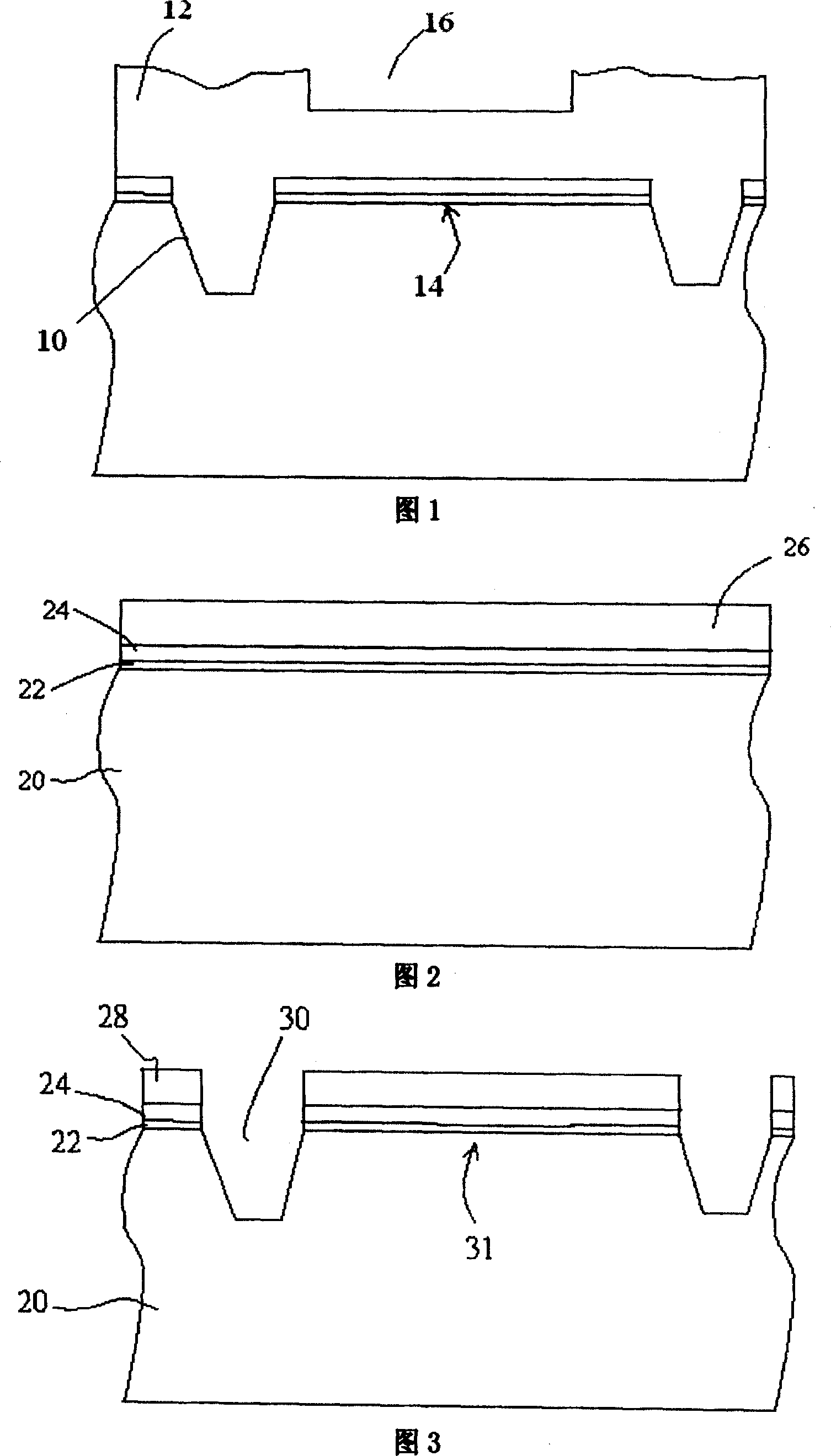
[0004] However, referring to the shallow trench isolation structure shown in FIG. 1, it is often easy to cause uneven density of oxide 12 filled in the trench 10 due to the increase in the aspect ratio of the trench 10, so it is necessary to set a dummy active in the trench. region (dummy active area) (not shown in the figure), and when the active region 14 on the semiconductor substrate has a larger area or a higher active region density, in order to remove the oxidation outside the trench 10 in the subsequent To obtain a more uniform polishing rate, it is necessary to use a reverse mask to form a groove 16 on the oxide layer 12 on the active region 14 with a larger area, so that uniform polishing can be obtained when the surface is planarized speed, but the formation of grooves 16 on a large-area or high-density active region 14 tends to easily lead to a decrease in the density of the oxide layer 12 of the active region 14, resulting in poor polishing rates and the like

Method used


Image

  • Improvement for shallow slot separated structure height homogeneity
  • Improvement for shallow slot separated structure height homogeneity
  • Improvement for shallow slot separated structure height homogeneity

Examples


Embodiment Construction

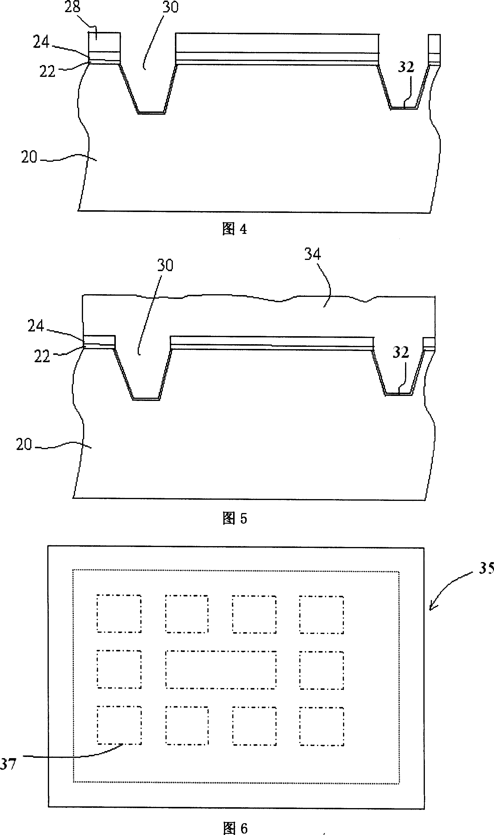
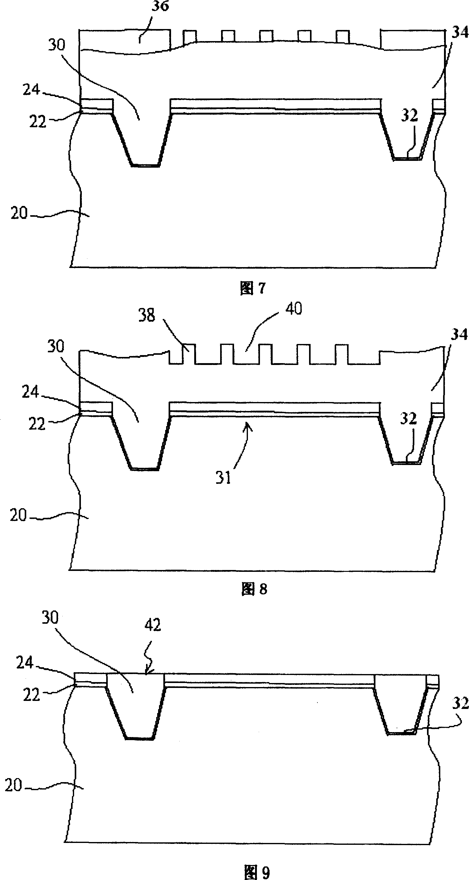
[0017] The invention relates to a method for improving the height uniformity of the shallow trench isolation structure, which can be widely applied to the isolation process in the deep submicron semiconductor process to obtain the best isolation effect between elements. Referring to Fig. 2, at first a semiconductor substrate 20 is provided, then the semiconductor substrate 20 is cleaned, then the semiconductor substrate 20 after cleaning is sent into a vertical or horizontal furnace tube, in an oxygen-containing environment, On the semiconductor substrate 20, a material is formed as a pad oxide layer 22 of silicon dioxide (SiO2), a material is a nitride layer 24 of silicon nitride (Si3N4) made by a low pressure chemical vapor deposition method, and a photo The resist layer 26 is then transferred to the photoresist with an active area (Active Area) mask (not shown in the figure) to form a first patterned photoresist. Layer 28, as shown in FIG. 3, is then anisotropic etched (Ani...


PUM


Abstract

When oxide layer locating out of shallow-trench is removed, complex number of arrayed oxide columns and oxide holes are formed on oxide layer on active region in order to acquire optimal polishing speed balance point when CMP crafts is made for semiconductor substrate with larger active region and higher density.

Description

technical field [0001] The invention relates to a method for manufacturing a shallow trench isolation structure, in particular to a method for improving the height uniformity of the shallow trench isolation structure. Background technique [0002] After decades of development in the integrated circuit industry, people have been able to put tens of millions of transistors on a chip with an area of ​​only 2 to 3 square centimeters. However, to place such a large number of IC components on such a small-sized chip, how to isolate the components to prevent mutual interference is a major technical focus. More importantly, the current component size is developing towards deep submicron. It has become an inevitable trend, so the importance of the isolation process is becoming more and more significant. [0003] There are two ways to use the isolation process on integrated circuits, one is local oxidation of silicon, and the other is shallow trench isolation process (Shallow trench ...

Claims


Application Information

Patent Timeline
IPC IPC(8): H01L21/76
Inventor 孔蔚然
Owner GRACE SEMICON MFG CORP
Learn More