Electronic device and method for manufacturing this device

A technology of electronic devices and electrode holders, which is applied in the direction of circuits, electrical components, and electrical solid devices, and can solve problems such as poor connection, large volume of anisotropic conductive resin, and detachment of button bumps

Inactive Publication Date: 2002-03-20
RENESAS ELECTRONICS CORP
View PDF1 Cites 6 Cited by
  • Summary
  • Abstract
  • Description
  • Claims
  • Application Information

AI Technical Summary

Problems solved by technology

However, in this case, for a semiconductor chip having a large stud bump height, the volume of the anisotropic conductive resin interposed between the semiconductor chip and the wiring board becomes large, thereby possibly producing a poor connection so that it is not affected by heat. Lower button tab disengages connection section of terminal block

Method used


Image

  • Electronic device and method for manufacturing this device
  • Electronic device and method for manufacturing this device
  • Electronic device and method for manufacturing this device

Examples


Embodiment Construction

[0062] Embodiments of the present invention will be described in detail below with reference to the accompanying drawings. In all the drawings for explaining the embodiments, parts having the same functions are identified by the same reference numerals so that their repeated descriptions will be omitted.

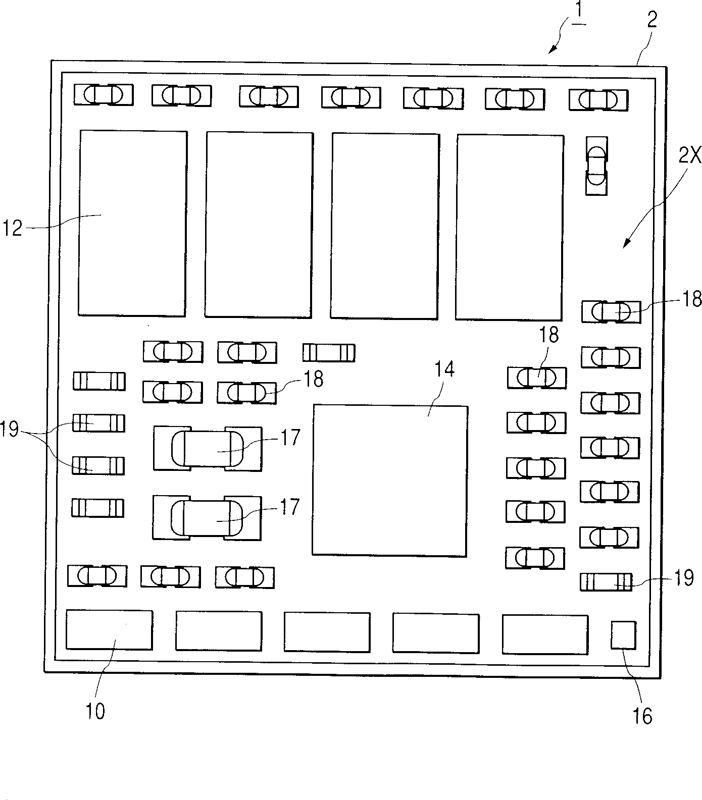
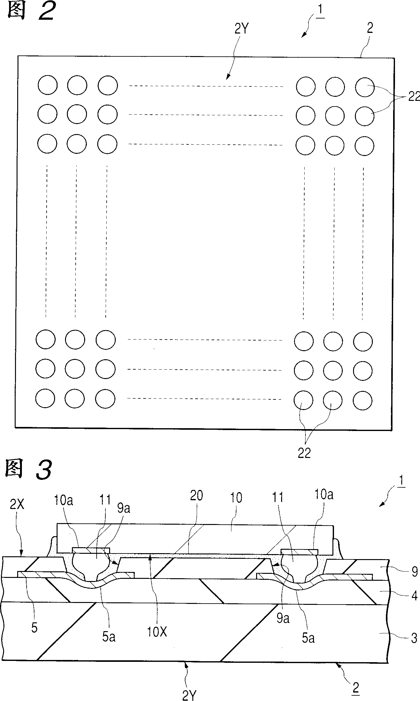
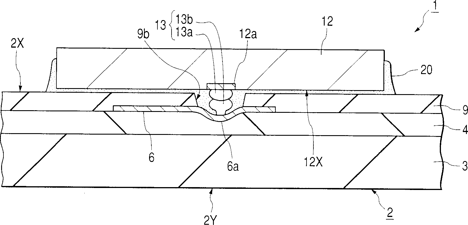
[0063] figure 1 is a schematic plan view of an MCM (an electronic device) according to a first embodiment of the present invention, FIG. 2 is a bottom view of the MCM, and FIG. figure 1 Schematic cross-sectional view of the assembled state of a buffer chip in the MCM, Figure 4 is a representation included in figure 1 A schematic cross-sectional view of the assembled state of a memory chip in the MCM, Figure 5 is a representation included in the figure 1 A schematic cross-sectional view of the assembled state of a controller chip in the MCM, Figure 6 is a representation included in the figure 1 A schematic cross-sectional view of the assembled state of a capacitor i...


PUM


Abstract

An electronic device comprising: a semiconductor chip having plural electrode pads on one main surface thereof; a wiring board having plural connection parts; and plural salient electrodes disposed respectively between the electrode pads of the semiconductor chip and the connection parts of the wiring board to provide electrical connections between the two, the salient electrodes being arranged in an array not providing balance of the semiconductor chip with respect to one main surface of the wiring board, the plural connection parts of the wiring board being arranged at a deeper position than one main surface of the wiring board in a depth direction from the one main surface.

Description

technical field [0001] The invention relates to an electronic device and a method for making the device. In particular, the present invention relates to a technology that is effectively applicable to electronic devices employing flip-chip mounting (mounting) technology. Background technique [0002] An electronic device called an MCM (Multi-Chip Module) is known as an electronic device. In an MCM, a plurality of semiconductor chips each including an integrated circuit are mounted on a wiring board to perform an integrated function. Regarding MCMs, it is becoming more and more popular to employ a flip-chip mounting technique in which a semiconductor chip (flip-chip) with raised electrodes formed on electrode pads on a circuit-forming surface is mounted on the terminal block. This is to increase data transfer speed and reduce device size. [0003] Regarding flip chip mounting technology, various mounting methods have been proposed and put to practical use. For example, as...

Claims


Application Information

Patent Timeline
Patent Type & Authority Applications(China)
IPC IPC(8): H01L25/18H01L21/56H01L21/60H01L23/498H01L25/04
CPCH01L2224/73203H01L2924/0105H01L24/17H01L2924/15747H01L2924/1517H01L2224/05567H01L2924/0132H01L2224/0401H01L2924/19041H01L2224/06136H01L2924/01013H01L2924/01039H01L2224/16238H01L2224/32225H01L2924/0665H01L2224/2919H01L2224/2929H01L21/563H01L24/06H01L2924/19043H01L2224/1134H01L2224/73204H01L2224/838H01L24/83H01L2924/01033H01L24/31H01L2224/16227H01L2224/16225H01L24/12H01L2924/01082H01L2924/0781H01L2924/01004H01L2224/16237H01L2224/83101H01L2224/29386H01L2224/13144H01L2924/01029H01L2924/00013H01L2224/29111H01L2224/293H01L24/11H01L2924/014H01L2924/30107H01L2224/81191H01L2224/05571H01L23/49816H01L2924/01079H01L2224/1308H01L24/16H01L2224/04042H01L2924/14H01L24/29H01L2924/01005H01L2924/01006H01L2924/01014H01L2224/131H01L2224/8319H01L2224/29299H01L2924/0002H01L2224/45144H01L2224/13023H01L2924/00014H01L2224/13099H01L2924/00H01L2924/00012H01L2224/13111H01L2924/05442H01L2224/29099H01L2224/29199H01L2224/05552H01L21/60
Inventor 今须诚士吉田育生岸川笵夫角义之田口一之内藤孝洋佐藤俊彦
Owner RENESAS ELECTRONICS CORP
Why Eureka
Try Eureka