Method for producing high accuracy delayed signal by using multiple signal source and its device

A delay signal and multiple signal technology, applied in the direction of generating/distributing signals, etc., can solve problems such as insurmountable, low error range, and difficult time control, etc., to solve the problem of unsynchronized, high precision, and adjustable delay time Effect

Inactive Publication Date: 2003-04-23
TIAN HLDG
View PDF0 Cites 0 Cited by
  • Summary
  • Abstract
  • Description
  • Claims
  • Application Information

AI Technical Summary

Problems solved by technology

see again Figure 1B If it is required to input the second cross-chip signal 12 to the third chip C3 after a time length of t13, it must keep synchronization with the third cross-chip signal or maintain a certain time interval (for example, Figure 1B During the time length marked t23), because the second cross-chip signal 12 is generated by the first chip C1 after passing through the second chip C2, so in terms of actual implementation experience, the second cross-chip signal is really The time of transmission to the third chip C3 is not easy to grasp. The reason is that at least it includes output pad delay (PAD delay) or circuit board delay (PCB delay) and other process or layout design uncertain factors.
[0004] Based on this, the existing attempt is to set a delay cell (delay cell) (because it is a prior art, so it is not shown in FIG. 1 ) to generate a fixed delay signal into the first chip C1, and make the first chip C1 The method of delaying the chip C1 for a fixed time length t12 before generating and outputting the second cross-chip signal to the third chip C3 obviously cannot overcome the uncertain factors in the manufacturing process or layout design for the second cross-chip signal The impact of maintaining synchronization with the third cross-chip signal or maintaining a certain time off
This situation will be more serious in the high-frequency working environment, that is, once the uncertain factors in the process or layout design cause the gap between the second cross-chip signal and the third cross-chip signal When the time difference deviates from the original design, because the acceptable error range is low in the high-frequency working environment, this display will easily cause the third chip C3 to malfunction

Method used


Image

  • Method for producing high accuracy delayed signal by using multiple signal source and its device
  • Method for producing high accuracy delayed signal by using multiple signal source and its device
  • Method for producing high accuracy delayed signal by using multiple signal source and its device

Examples


Embodiment Construction

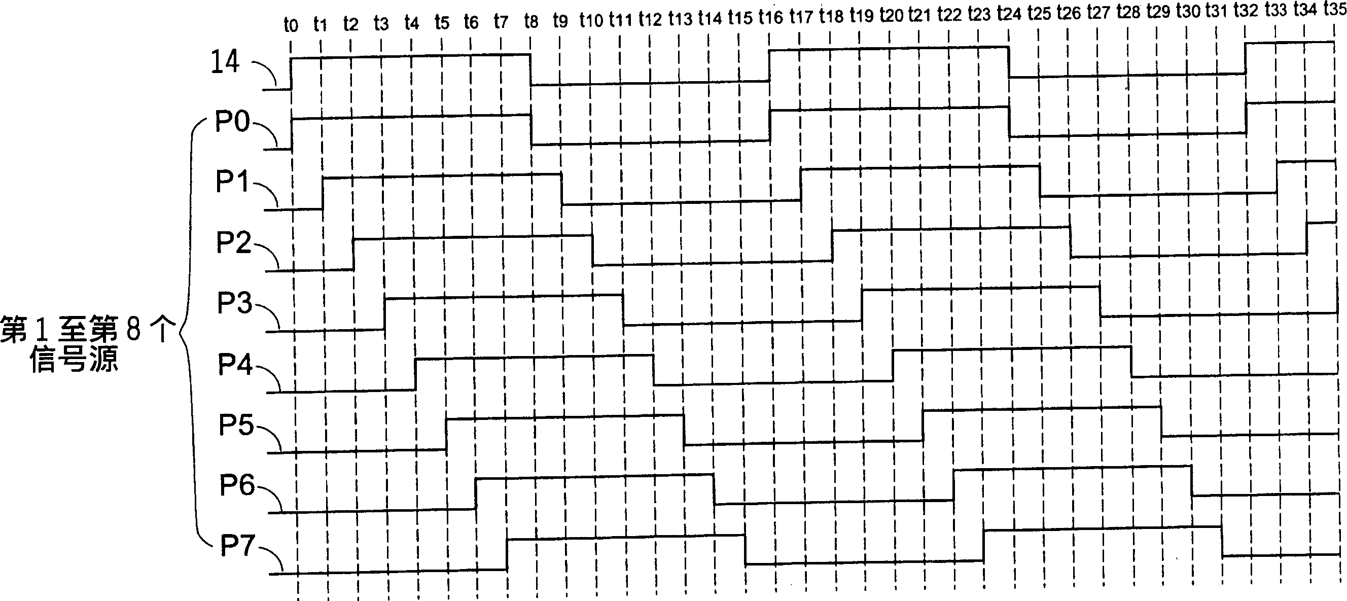
[0055] Such as Figure 2A As shown, it is a conceptual example diagram of generating multiple signal sources (multiplesignal source) in the preferred implementation method of this case; that is, in Figure 2A Among them, a high-frequency signal can be used to generate multiple signal sources (for example, the 1st to 8th signal sources P0-P7); wherein, any two adjacent signal sources differ by one clock period; and, the The 8 signal sources P0~P7 can be 8 locks produced by a phase-locked loop (Phase-Locked Loop, PLL) device (because it is prior art, so Fig. 2 does not show) that inputs this high-frequency signal phase loop signal.

[0056] Such as Figure 2B shown, for the use of Figure 2A The waveform diagram of the multiple signal sources to generate the delayed signal is shown in . exist Figure 2B In t1 and t3, the signal sources P1 and P3 are respectively selected for output, so that the first and second output signals 21 and 22 respectively produce a level state tra...


PUM


Abstract

The method for producing high-accuracy delayed signal by using multiple signal source includes the following steps: providing several signal sources; in which between any two adjacent signal sources its difference is a clock period; responsing said several signal sources to respectively produce first and second output signals in first and second times; making said output signals undergo the process of one logic operation treatment to obtain a delay signal. At the same time said invention also provides an aquipment for implementing said method. Said equipment includes a multiple signal soruce generation device, a signal source output selection device and a logic operation device.

Description

technical field [0001] The present invention relates to a method and device for generating delayed signals, especially to a method and device for generating high-precision delayed signals with multiple signal sources in a high-frequency working environment. Background technique [0002] As the working speed of the microprocessor becomes faster and faster, more and more problems are brought about in its design; among them, the signal synchronization problem between chips is an important subject to be solved at present. [0003] see Figure 1A , Figure 1B , respectively are an example diagram of a chip architecture taking three chips as an example and a schematic diagram of a comparison of signal waveforms. exist Figure 1A Among them, 10 is a delayed signal. In addition to directly generating the third cross-chip signal 13 for use by the third chip C3, the first chip C1 can also indirectly generate the first cross-chip signal 11 to the second chip C2, so that The second ch...

Claims


Application Information

Patent Timeline
Patent Type & Authority Applications(China)
IPC IPC(8): G06F1/04
Inventor 庄英朗
Owner TIAN HLDG
Why Eureka
Try Eureka