Semiconductor storage device and information apparatus

A semiconductor and device technology, applied in the field of non-volatile memory, can solve the problems of time consumption and long extra time, and achieve the effect of high-speed data readout

Inactive Publication Date: 2003-07-02
SAMSUNG ELECTRONICS CO LTD
View PDF0 Cites 5 Cited by
  • Summary
  • Abstract
  • Description
  • Claims
  • Application Information

AI Technical Summary

Problems solved by technology

[0055] However, if unwanted data is once output immediately after the sensing start time (time t(a)), in many cases, additional time is consumed until desired data is successfully output.
This extra time

Method used


Image

  • Semiconductor storage device and information apparatus
  • Semiconductor storage device and information apparatus
  • Semiconductor storage device and information apparatus

Examples


Embodiment Construction

[0092] Detailed description of the preferred embodiment

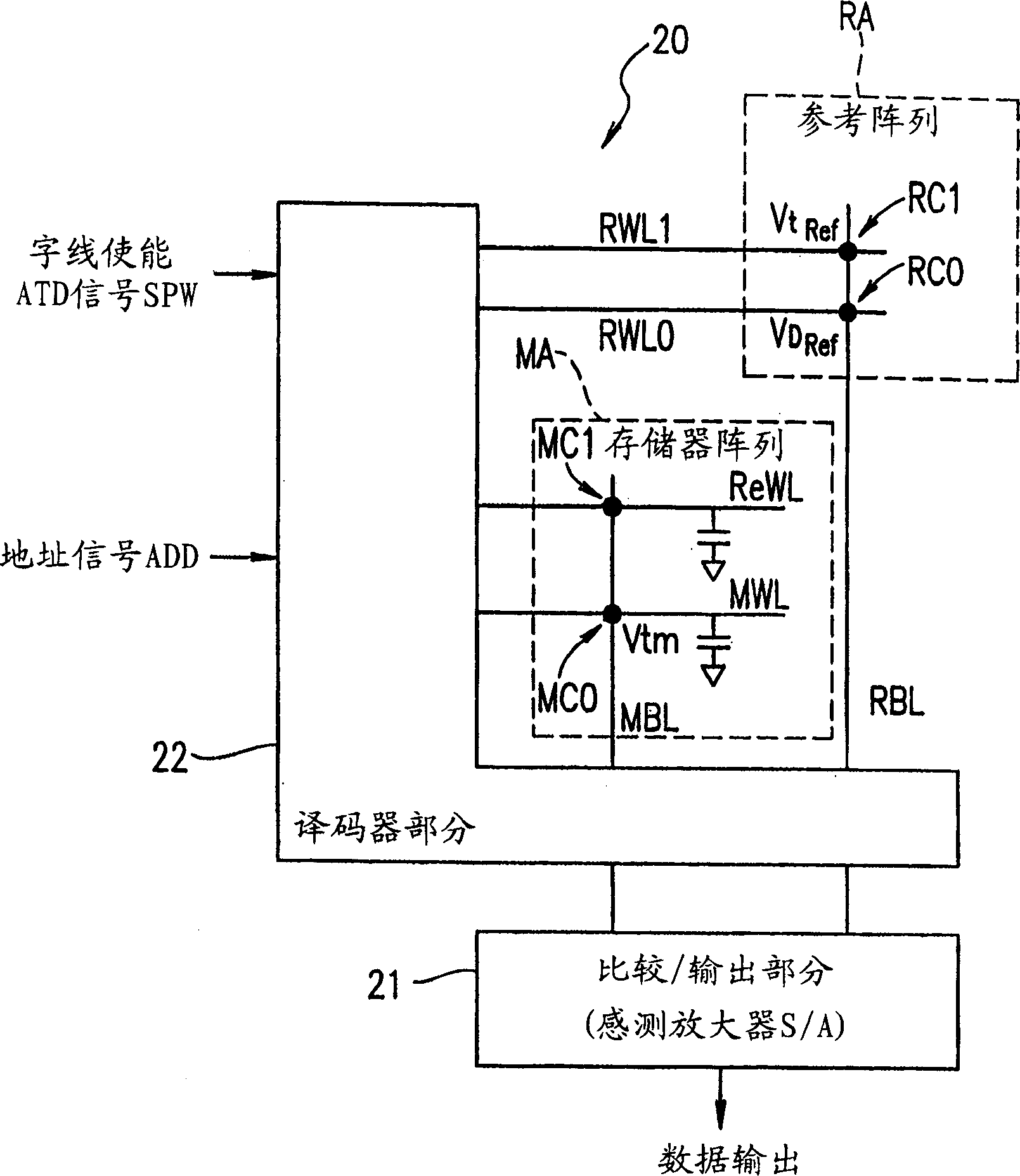
[0093] Hereinafter, embodiments of the present invention will be described with reference to the drawings. In the embodiments described below, the present invention is applied to nonvolatile semiconductor devices used in information equipment.

[0094] figure 1 is a block diagram showing an exemplary basic structure of a nonvolatile semiconductor storage device according to an embodiment of the present invention.

[0095] exist figure 1 Above, the nonvolatile semiconductor storage device 20 includes: a memory cell array RA (hereinafter referred to as "reference array RA") having a plurality of reference cells RC0 and RC1; a memory cell array MA (hereinafter referred to as "memory array MA") , which is a data storage area and is the main array of storage devices 20; a comparison / output section 21, such as a sense amplifier S / A formed by a differential amplifier; and a decoder section 22, for selecting according to a...


PUM


Abstract

A semiconductor storage device includes: a memory array including a plurality of memory cells; a reference array including a plurality of reference cells; a decoder section for selecting a memory cell from the memory cells and a reference cell from the reference cells based on address information; and a comparison/output section for comparing a read voltage level from the memory cell selected by the decoder section and a read voltage level from the reference cell selected by the decoder section so as to output a result of the comparison in the form of data, wherein the decoder section simultaneously outputs a selection signal to a word line of the memory cell and a selection signal to a word line of the reference cell.

Description

technical field [0001] The present invention relates to a nonvolatile memory in which data is electrically writable (for example, a semiconductor storage device such as flash EEPROM, etc.), and to information equipment using the nonvolatile memory, such as a cellular phone terminal and the like. Background technique [0002] Conventionally, in a nonvolatile semiconductor storage device (nonvolatile memory such as flash EEPROM) in which data is electrically writable, a data read operation is performed as follows: Figure 8 As shown, the same drain voltage is applied to the memory cell RC0 (which is called a "reference cell") set at a predetermined threshold value, and to the memory cell MC0 of the memory array on which the data read operation is performed. , while the same gate voltage is applied by the reference word line decoder and the normal word line decoder, and the difference between the current values ​​flowing through the memory cells RC0 and MC0 is sensed by the sens...

Claims


Application Information

Patent Timeline
IPC IPC(8): G11C16/06G11C8/08G11C16/02G11C16/04G11C16/08G11C16/28G11C29/24
CPCG11C8/08G11C16/28G11C16/08
Inventor 山野要
Owner SAMSUNG ELECTRONICS CO LTD
Why Eureka
Try Eureka