Method of forming phsical gas phase deposition target contg. aluminium, sputtering film and component of target

A physical vapor deposition, aluminum block technology, used in sputtering, vacuum evaporation, coating, etc., can solve the problem of difficult to eliminate, can not produce small grain size microstructure, can not form less than 150 microns thermally stable crystal. particle size, etc.

Inactive Publication Date: 2003-07-23
HONEYWELL INT INC
View PDF5 Cites 47 Cited by
  • Summary
  • Abstract
  • Description
  • Claims
  • Application Information

AI Technical Summary

Problems solved by technology

[0014] For the above reasons, conventional metal treatment processes cannot produce the small grain size and stable microstructure required for high-purity aluminum targets for flat panel display technology
For example, a problem with conventional deformation techniques is that high-purity metals typically cannot form thermally stable grain sizes of less than 150 microns under doped and undoped conditions
These defects are difficult, if not impossible, to remove by cold deformation, and some of them are even worse during cold deformation

Method used


Image

  • Method of forming phsical gas phase deposition target contg. aluminium, sputtering film and component of target
  • Method of forming phsical gas phase deposition target contg. aluminium, sputtering film and component of target
  • Method of forming phsical gas phase deposition target contg. aluminium, sputtering film and component of target

Examples


Embodiment 1

[0077] Example 1: High purity aluminum doped with 30 ppm Si processed according to the method of the present invention.

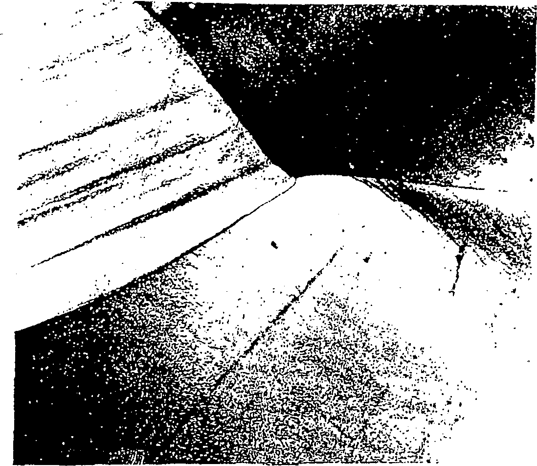
[0078] Cast material defined as 5N5Al and 30ppm Si was processed by 75% hot forging deformation and 6 passes through ECAE along path D. This material with a grain size of 15 μm has a fully recrystallized structure. Subsequent rolling with a deformation of 85% grew the average grain size to 20 μm with an aspect ratio of about 1.5. Annealing at 150°C for 1 hour resulted in significant grain growth to 23 µm, which was estimated to be the maximum temperature expected in the subsequent sputtering process. During the long (16 hours) exposure to 150° C., the grains grew to 28 μm. Raising the temperature to 200° C. for 1 hour produced a similar grain size of about 30 μm. Therefore, the combination of ECAE and rolling makes the material structure of 5N5 Al plus 30ppm Si fine and uniform, and its average grain size is less than or equal to about 30μm, which is sta...

Embodiment 2

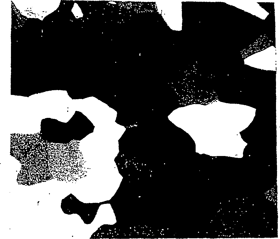
[0079] Example 2: High purity aluminum doped with 10 ppm Si processed according to the method of the present invention.

[0080] The sample was cast, 74% hot forged and subjected to 6 ECAE extrusions along path D. A fully dynamically recrystallized structure with an average grain size of about 19 μm was obtained after ECAE. Subsequent 85% rolling and annealing at 150° C. for 1 hour resulted in fully recrystallized grain sizes of approximately 35 μm.

Embodiment 3

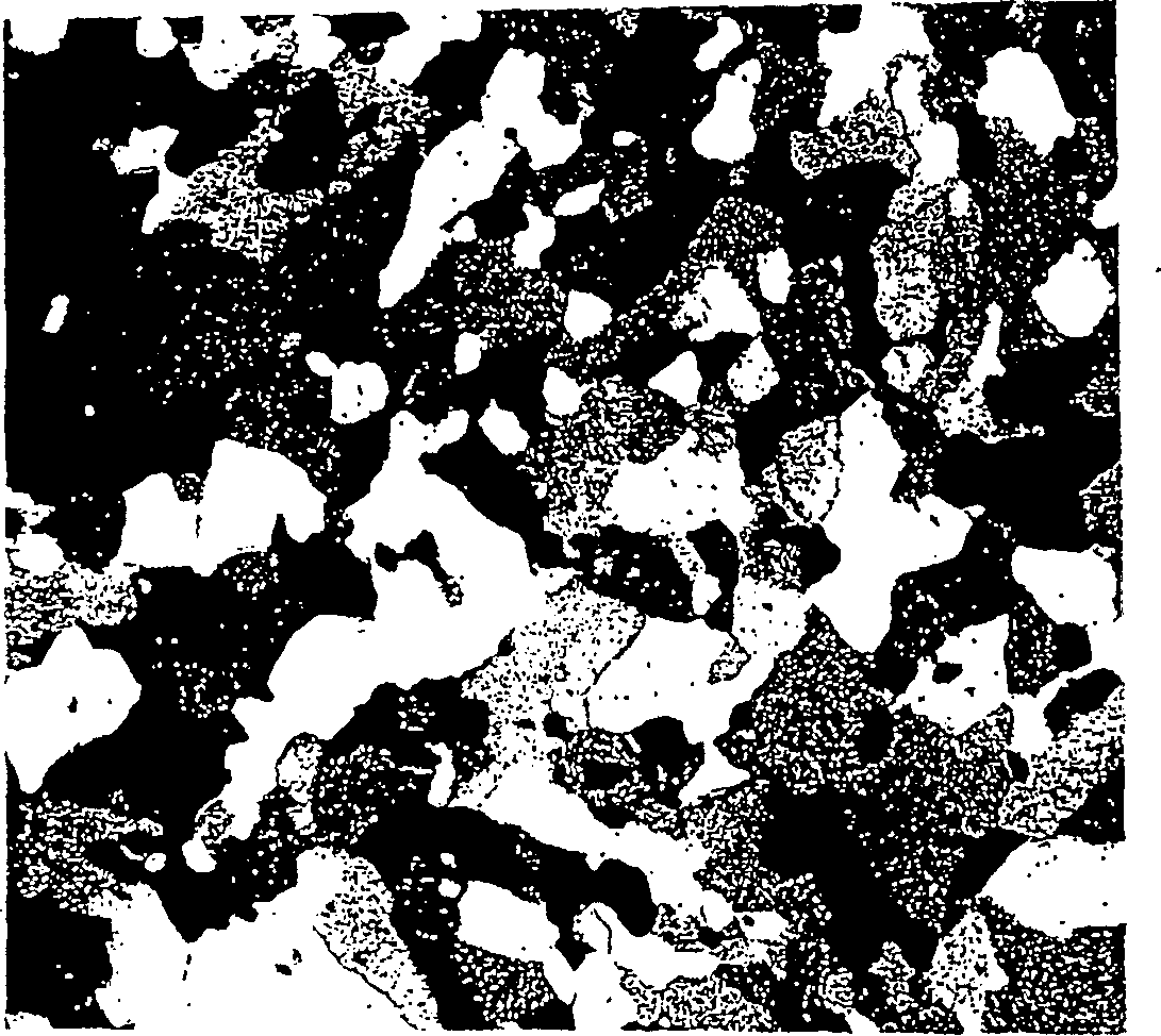
[0081] Example 3: High purity aluminum doped with 10 ppm Sc processed according to the method of the present invention.

[0082] The sample was cast, 74% hot forged and subjected to 6 ECAE extrusions along path D. A fully dynamically recrystallized structure with an average grain size of about 26 μm was obtained after ECAE. During rolling deformation up to 60%, the structure remains stable and remains typical of re-rolled materials. After 70% deformation, the first recrystallized grains were observed. After 85% rolling deformation, about 60% of the sample area was fully recrystallized to an average grain size of about 45 μm.


PUM

PropertyMeasurementUnit
sizeaaaaaaaaaa
sizeaaaaaaaaaa

Abstract

The invention includes a method of forming an aluminum-comprising physical vapor deposition target. An aluminum-comprising mass is deformed by equal channel angular extrusion. The mass is at least 99.99% aluminum and further comprises less than or equal to about 1,000 ppm of one or more dopant materials comprising elements selected from the group consisting of Ac, Ag, As, B, Ba, Be, Bi, C, Ca, Cd, Ce, Co, Cr, Cu, Dy, Er, Eu, Fe, Ga, Gd, Ge, Hf, Ho, In, Ir, La, Lu, Mg, Mn, Mo, N, Nb, Nd, Ni, O, Os, P, Pb, Pd, Pm, Po, Pr, Pt, Pu, Ra, Rf, Rh, Ru, S, Sb, Sc, Se, Si, Sm, Sn, Sr, Ta, Tb, Te, Ti, Tl, Tm, V, W, Y, Yb, Zn and Zr. After the aluminum-comprising mass is deformed, the mass is shaped into at least a portion of a sputtering target. The invention also encompasses a physical vapor deposition target consisting essentially of aluminum and less than or equal to 1,000 ppm of one or more dopant materials comprising elements selected from the group consisting of Ac, Ag, As, B, Ba, Be, Bi, C, Ca, Cd, Ce, Co, Cr, Cu, Dy, Er, Eu, Fe, Ga, Gd, Ge, Hf, Ho, In, Ir, La, Lu, Mg, Mn, Mo, N, Nb, Nd, Ni, O, Os, P, Pb, Pd, Pm, Po, Pr, Pt, Pu, Ra, Rf, Rh, Ru, S, Sb, Sc, Se, Si, Sm, Sn, Sr, Ta, Tb, Te, Ti, Tl, Tm, V, W, Y, Yb, Zn and Zr. Additionally, the invention encompasses thin films.

Description

field of invention [0001] The present invention relates to a method of forming an aluminum-containing physical vapor deposition target and the composition of the target. In a particular application, the invention relates to the deformation of aluminum-containing blocks using equal channel angular extrusion (ECAC) to form physical vapor deposition (PVD )target. Background of the invention [0002] PVD is a technique for sputter depositing thin metal and / or ceramic layers onto a substrate. The sputtered material comes from a target that is typically used as the cathode in standard radio frequency (RF) and / or direct current (DC) sputtering equipment. For example, PVD is widely used in the semiconductor industry to fabricate integrated circuits. [0003] A newer application of sputtering technology is the fabrication of FPDs, such as LCDs. The LCD market has experienced rapid growth. This trend will accelerate in the next few years due to the diverse applications of LCDs in...

Claims


Application Information

Patent Timeline
Patent Type & Authority Applications(China)
IPC IPC(8): B21C23/00C22C21/00C22F1/00C22F1/04C23C14/34
CPCC22F1/04C23C14/3414Y10S72/70C23C14/14
Inventor V·M·赛加尔J·李F·E·沃福德S·费尔拉斯
Owner HONEYWELL INT INC
Why Eureka
Try Eureka