Method of depositing nanolaminate film for non-volatile floating gate memory devices by atomic layer deposition

a technology of floating gate memory and nanolaminate film, which is applied in the direction of semiconductor devices, semiconductor/solid-state device details, electrical devices, etc., can solve the problems of difficult formation of uniform size and density over a large area, difficult to form a thin film with uniform size and density, and difficult to form a thin film than when using chemical vapor deposition

Inactive Publication Date: 2008-03-06
KOREA RES INST OF CHEM TECH
View PDF2 Cites 412 Cited by
  • Summary
  • Abstract
  • Description
  • Claims
  • Application Information

AI Technical Summary

Benefits of technology

[0014] The present inventors have made many efforts to achieve the above objects and, as a result, were able to depositing a nanolaminate film of first high-dielectric-constant layer / nickel oxide layer / second high-dielectric-constant layer for non-volatile floating gate memory devices through a method comprising forming a first high-dielectric-constant layer on a substrate using the ALD method, alternately supplying a nickel source and an oxygen source on the first high-dielectric-constant layer using the ALD method so as to form a nickel oxide layer, which can be controlled to a given thickness, and then forming on the nickel oxide layer a second-high-dielectric-constant layer using the ALD method, and found that the nanolaminate film of first high-dielectric-constant layer / nickel oxide layer / second high-dielectric-constant layer, deposited using said method, shows good memory window (threshold voltage) characteristics when it is applied to non-volatile floating gate memory devices, thereby completing the present invention.

Problems solved by technology

However, such methods employing nanocrystals have a problem in that nanocrystals, which play an important role in device characteristics, are difficult to form with uniform size and density over a large area.
In the physical vapor deposition, the surface of a grown thin film is rough, and it is not easy to grow a uniform thin film on a large-area substrate or a three-dimensional substrate, and it is more difficult to form a thin film than when using the chemical vapor deposition.
However, there is, so far, no example in which the NiO thin film grown using the ALD method is applied to non-volatile floating gate memory devices.

Method used


Image

  • Method of depositing nanolaminate film for non-volatile floating gate memory devices by atomic layer deposition
  • Method of depositing nanolaminate film for non-volatile floating gate memory devices by atomic layer deposition
  • Method of depositing nanolaminate film for non-volatile floating gate memory devices by atomic layer deposition

Examples


example 1

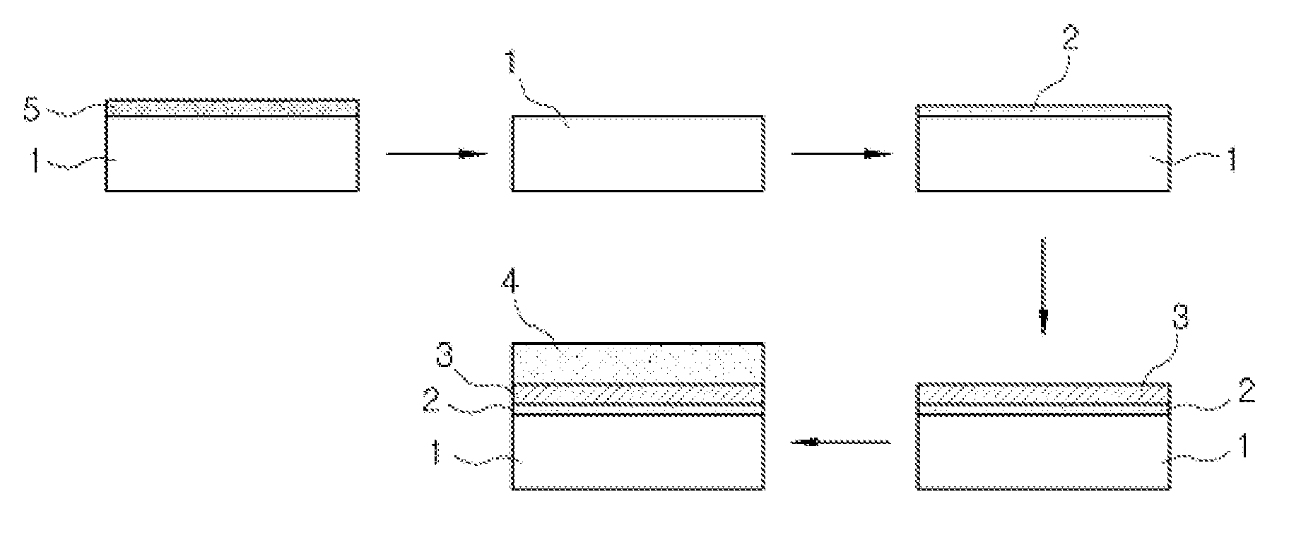
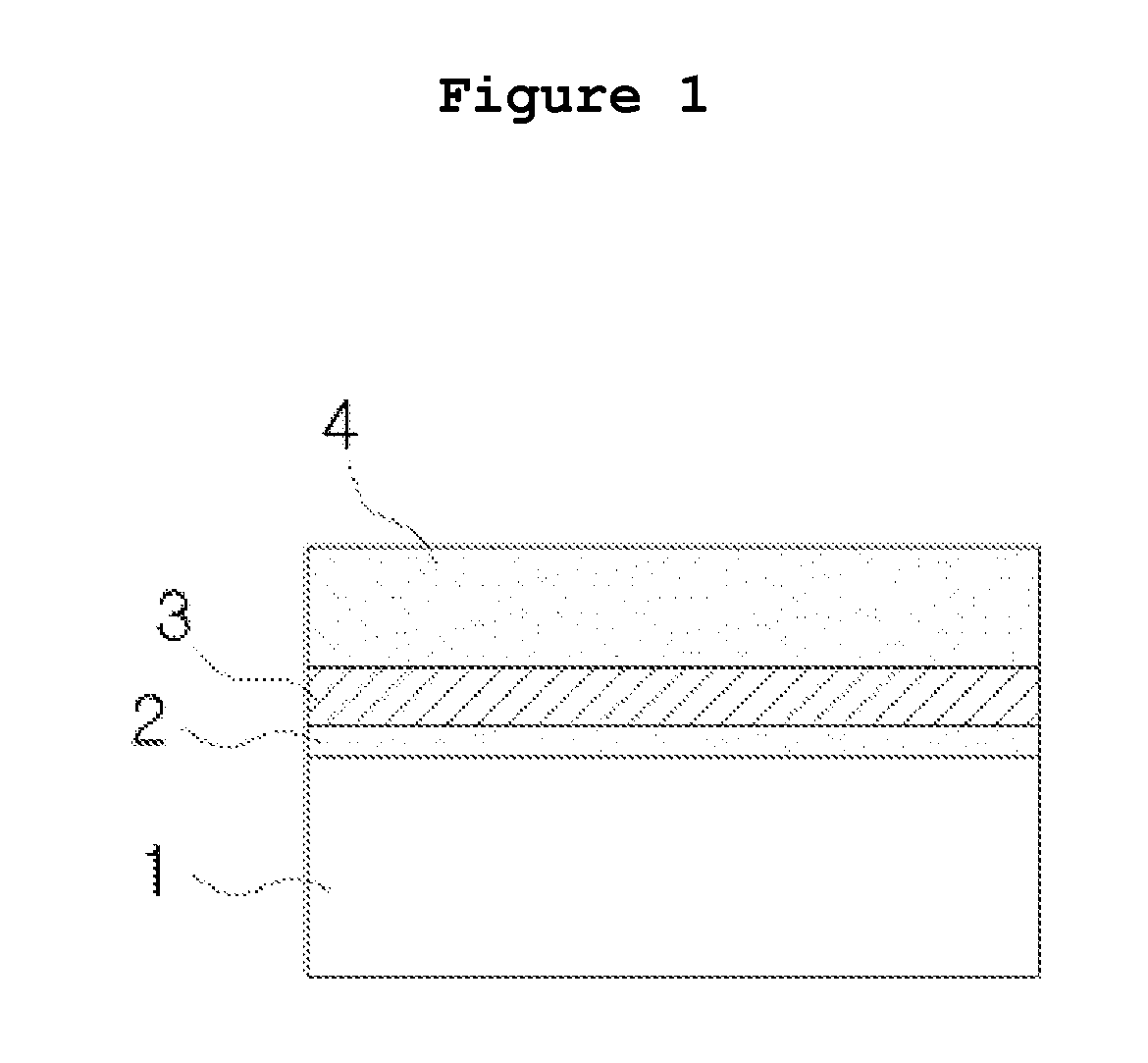
[0061]FIG. 2 is a schematic diagram showing a process of depositing an Al2O3 / NiO / Al2O3 nanolaminate film according to the present invention. The nanolaminate film was deposited using the process sequence shown in FIG. 2.

[0062] Specifically, a silicon substrate to be deposited with an Al2O3 / NiO / Al2O3 film was washed sequentially with acetone, ethanol and deionized water, and then cleaned with an HF-containing cleaning solution to remove native oxides from the surface of the silicon substrate, followed by washing with deionized water. Then, the silicon substrate was placed in an atomic layer deposition reactor, which was vented with an evacuation pump, and the temperature of the substrate was controlled to 120° C.

[0063] Then, an Al2O3 layer was formed on the silicon substrate using trimethyl aluminum and water. Herein, the aluminum source and water were maintained at room temperature, and the formation of the Al2O3 layer was carried out in the following conditions: flow rate of purg...

example 2

[0067] Al2O3 / NiO / Al2O3 nanolaminate films were deposited in the same conditions as in Example 1, except that the thickness of the NiO layer was changed to 3 nm, 5 nm and 8 nm. Then, a 300-μm thick Al electrode was formed on each of the nanolaminate films. Memory window (threshold voltage shift) values at the NiO thicknesses were measured, and the measurement results are shown in FIG. 3. As can be seen from the results in FIG. 3, the memory window of the non-volatile floating gate memory device was large, even when the NiO thickness thereof was 3 nm. Also, there was little or no difference in memory window between NiO thicknesses of 5 nm and 8 nm, even though the memory window became larger with an increase in NiO thickness.

example 3

[0068] An Al2O3 / NiO / Al2O3 nanolaminate film deposited under the same conditions as in Example 1 was measured for memory window (threshold voltage shift) at varying sweep voltages, and the measurement results are shown in FIG. 4. As can be seen from the results in FIG. 4, the memory window became larger as the sweep voltage increased from ±2.5 V to ±5.0 V and ±7.0V.

[0069] From the results in FIGS. 3 and 4, it can be seen that the nanolaminate film according to the present invention has good memory window characteristics, such that it can be applied to non-volatile floating gate memory devices.

[0070] As described above, the inventive method of depositing a nanolaminate film of first high-dielectric-constant layer / nickel oxide layer / second high-dielectric-constant layer by atomic layer deposition has advantages in that it can be carried out at a lower temperature than the prior physical deposition method, and it is very easy to control thickness, even in the case of very thin films. ...


PUM

PropertyMeasurementUnit
temperatureaaaaaaaaaa
dielectric constantaaaaaaaaaa

Abstract

Disclosed herein is a method of depositing a nanolaminate film for next-generation non-volatile floating gate memory devices by atomic layer deposition. The method includes the steps of: introducing a substrate into an atomic layer deposition reactor; forming on the substrate a first high-dielectric-constant layer by alternately supplying an oxygen source and a metal source selected from among an aluminum source, a zirconium source and a hafnium source; forming on the first high-dielectric-constant layer a nickel oxide layer by alternately supplying a nickel source and an oxygen source; and forming on the nickel oxide layer a second high-dielectric-constant layer by alternately supplying an oxygen source and a metal source selected from among an aluminum source, a zirconium source and a hafnium source. The nanolaminate film deposited according to the method shows good memory window characteristics compared to those of memory devices fabricated using nanocrystal floating gates according to the prior physical vapor deposition methods, and thus can be applied to non-volatile floating gate memory devices.

Description

CROSS-REFERENCE TO RELATED APPLICATION [0001] This application claims priority from and the benefit of Korean Patent Application No. 10-2006-83022, filed on Aug. 30, 2006, which is hereby incorporated by reference for all purposes as if fully set forth herein. BACKGROUND OF THE INVENTION [0002] 1. Field of the Invention [0003] The present invention relates to a method for depositing a nanolaminate film consisting of first high-dielectric-constant layer / nickel oxide layer / second high-dielectric-constant layer, which is to be used in non-volatile floating gate memory devices, by atomic layer deposition (ALD), and to a non-volatile floating gate memory device comprising the same. [0004] 2. Description of the Prior Art [0005] Memory devices, which have recently been increasingly used in mobile phones, MP3 players, digital cameras, USB devices, etc., are non-volatile memory devices that solve problems in the volatile operation mode of DRAM devices. As next-generation memory devices, non-...

Claims


Application Information

Patent Timeline
Patent Type & Authority Applications(United States)
IPC IPC(8): H01L29/788H01L21/31
CPCH01L21/02175H01L21/02178H01L21/02181H01L21/02189H01L21/3162H01L21/0228H01L21/28282H01L21/3142H01L21/022H01L29/40117H01L21/02107
Inventor KIM, CHANG-GYOUNLEE, YOUNG-KUKCHUNG, TAEK-MOAN, KI-SEOKLEE, SUN-SOOKCHO, WON-TAE
Owner KOREA RES INST OF CHEM TECH
Why Eureka
Try Eureka