Method for fabricating an ultralow dielectric constant material as an intralevel or interlevel dielectric in a semiconductor device and electronic device made

a technology of ultralow dielectric constant and semiconductor devices, which is applied in the direction of coatings, metallic material coating processes, chemical vapor deposition coatings, etc., can solve the problems of increasing signal delays in ulsi electronic devices, prohibitive mass production high cost of prior art precursor materials, etc., to achieve the effect of reducing tensile stress and cos

Inactive Publication Date: 2006-05-23
INTEL CORP
View PDF8 Cites 421 Cited by
  • Summary
  • Abstract
  • Description
  • Claims
  • Application Information

AI Technical Summary

Benefits of technology

[0014]The use of the first precursor that includes a silane derivative in combination with the second organic precursor enables an efficient incorporation of a pore forming phase in a SiCOH matrix and the preparation of SiCOH films at lower cost than with precursors described in the prior art.
[0015]The use of the first precursor that includes a silane derivative in combination with the second organic precursor can enable a porous SiCOH dielectric having a reduced tensile stress, according to the methods of this invention.

Problems solved by technology

This combined effect increases signal delays in ULSI electronic devices.
Most commercially available dielectric materials however are not thermally stable when exposed to temperatures above 300° C. Integration of low k dielectrics in present ULSI chips requires a thermal stability of at least 400° C.
Furthermore, these prior art precursor materials are high cost and prohibitive for use in mass production.

Method used


Image

  • Method for fabricating an ultralow dielectric constant material as an intralevel or interlevel dielectric in a semiconductor device and electronic device made
  • Method for fabricating an ultralow dielectric constant material as an intralevel or interlevel dielectric in a semiconductor device and electronic device made
  • Method for fabricating an ultralow dielectric constant material as an intralevel or interlevel dielectric in a semiconductor device and electronic device made

Examples


example 1

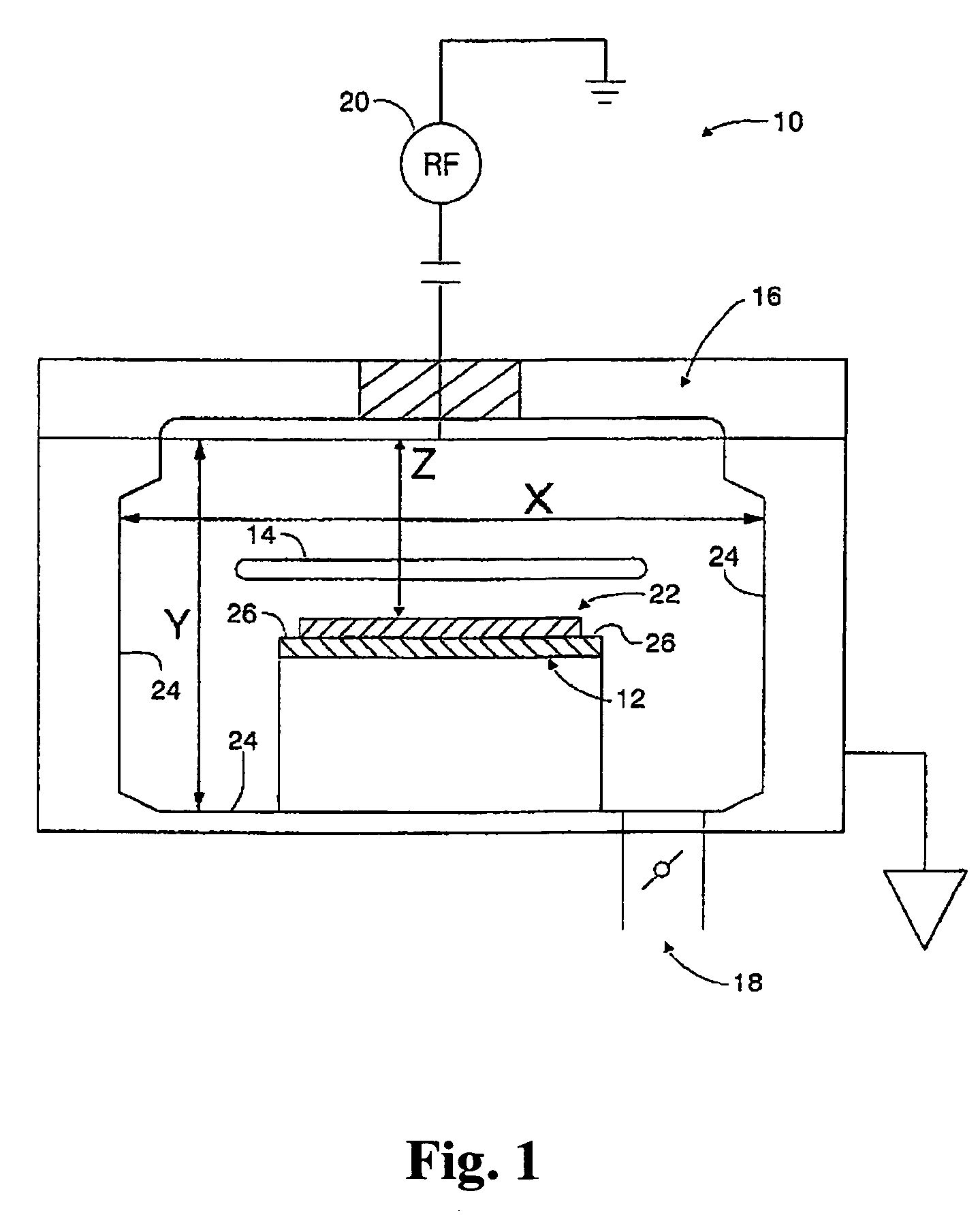
[0078]In this example, according to FIG. 1, a wafer was first prepared by introducing the wafer into reactor 10 through a slit valve 14 and the wafer was optionally pre-etched by argon gas. In this wafer preparation process, the wafer temperature was set at about 180° C. and the argon flow rate was set at about 25 sccm, to achieve a pressure of about 100 mtorr. A RF power was then turned on to about 125 W for about 60 seconds. The RF power and the argon gas flow were then turned off.

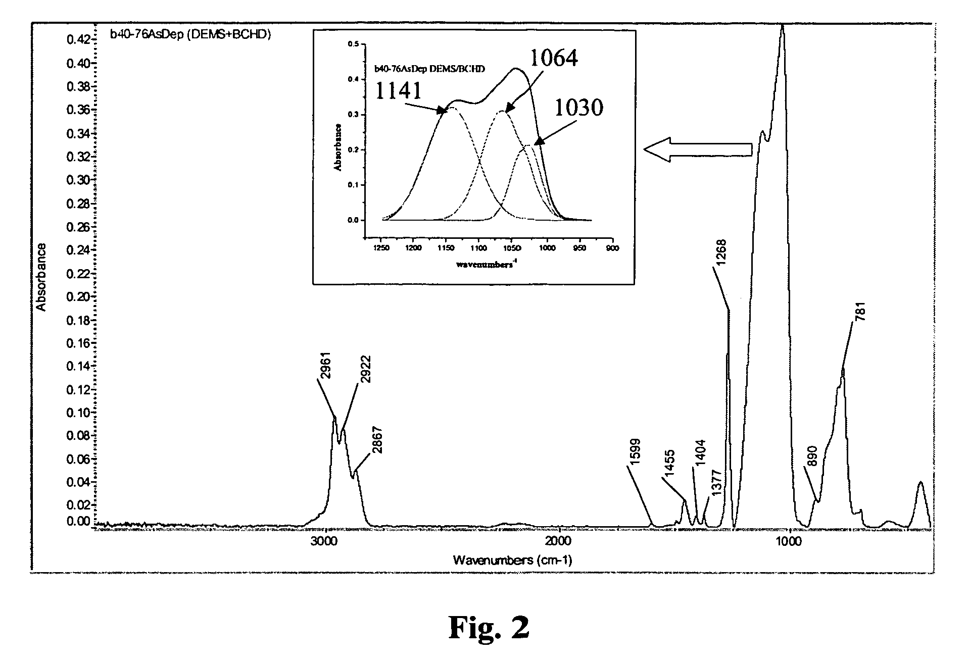
[0079]The DEMS precursor was carried into the reactor. The ultralow k film according to the present invention was deposited by first establishing gas flows of DEMS and BCHD to desired flow rates and pressure, i.e., at about 4 sccm of DEMS and about 3 sccm of BCHD and about 500 mtorr. A RF power was then turned on at about 30 W for a time period of about 50 minutes. The RF power and the gas flow were then turned off. The wafer was then removed from reaction reactor 10.

[0080]To reduce the dielectric consta...

example 2

[0082]In this example, a wafer was prepared in the same tool as in Example 1. The wafer was first introduced into the reaction chamber. The wafer temperature was set at about 180° C. The DEMS precursor was carried into the reactor. The ultralow k film according to the present invention was deposited by first establishing gas flows of DEMS and butadienemonoxide (BMO) to desired flow rates and pressure, i.e., at about 1 sccm of DEMS and about 4 sccm of BMO and about 500 mtorr. A RF power was then turned on at about 30 W for a time period of about 50 minutes. The RF power and the gas flow were then turned off. The wafer was then removed from reactor 10.

[0083]The film was then treated with the same method described in Example 1. The resulting film had a dielectric constant of 1.77.

example 3

[0084]In this example, a wafer was prepared in the same tool as in Example 1. The wafer was first introduced into the reaction chamber. The wafer temperature was set at about 180° C. The DEMS precursor was carried into the reactor. The ultralow k film according to the present invention was deposited by first establishing gas flows of DEMS and 2-methyl-2-vinyloxirane (MVOX) to desired flow rates and pressure, i.e., at about 2 sccm of DEMS and about 3 sccm of MVOX and about 500 mtorr. A RF power was then turned on at about 30 W for a time period of about 50 minutes. The RF power and the gas flow were then turned off. The wafer was then removed from reactor 10.

[0085]The film was then treated with the same method described in Example 1.

[0086]The resulting film had a dielectric constant of 2.08.


PUM

PropertyMeasurementUnit
temperatureaaaaaaaaaa
dielectric constantaaaaaaaaaa

Abstract

A method for fabricating a thermally stable ultralow dielectric constant film comprising Si, C, O and H atoms in a parallel plate chemical vapor deposition process utilizing a plasma enhanced chemical vapor deposition (“PECVD”) process is disclosed. Electronic devices containing insulating layers of thermally stable ultralow dielectric constant materials that are prepared by the method are further disclosed. To enable the fabrication of a thermally stable ultralow dielectric constant film, specific precursor materials are used, such as, silane derivatives, for instance, diethoxymethylsilane (DEMS) and organic molecules, for instance, bicycloheptadiene and cyclopentene oxide.

Description

CROSS-REFERENCE TO RELATED APPLICATIONS[0001]The present application is related to co-assigned U.S. Pat. Nos. 6,147,009, 6,312,793, 6,441,491, 6,437,443, 6,541,398, 6,479,110 B2, and 6,497,963, the contents of which are incorporated herein by reference in their entirety. The present application is also related to co-pending and co-assigned U.S. patent application Ser. No. 10 / 174,749, filed Jun. 19, 2002, Ser. No. 10 / 340,000, filed Jan. 23, 2003, Ser. No. 10 / 390,801, filed Mar. 18, 2003, and Ser. No. 10 / 758,724, filed Jan. 16, 2004, the contents of each of the aforementioned U.S. Patent Applications are also incorporated herein by reference in their entirety as well.FIELD OF THE INVENTION[0002]The present invention generally relates to a method for fabricating a dielectric material that has an ultralow dielectric constant (or ultralow k) and an electronic device containing such a dielectric material. More particularly, the present invention relates to a method for fabricating a therm...

Claims


Application Information

Patent Timeline
Patent Type & Authority Patents(United States)
IPC IPC(8): H01L21/31C23C16/40H01L21/312H01L21/316
CPCH01L21/02126H01L21/02216H01L21/02274H01L21/0234H01L21/31695H01L21/02351H01L21/02362H01L21/3122H01L21/31633H01L21/02348H01L21/02205H01L21/324
Inventor GATES, STEPHEN M.GRILL, ALFREDMEDEIROS, DAVID R.NEUMAYER, DEBORAHNGUYEN, SON VANPATEL, VISHNUBHAI V.WANG, XINHUI
Owner INTEL CORP
Why Eureka
Try Eureka