Correction circuit, delay circuit and annular oscillator circuit

A technology for calibrating circuits and circuits, applied in electrical pulse generator circuits, pulse manipulation delays, and logic circuits to generate pulses, etc., can solve problems such as inability to use, and achieve the effects of reducing power consumption and stabilizing delay time.

Inactive Publication Date: 2003-12-24
SHARP KK
View PDF1 Cites 6 Cited by
  • Summary
  • Abstract
  • Description
  • Claims
  • Application Information

AI Technical Summary

Problems solved by technology

Therefore, when the time period until this voltage is obtained from the standby-release state is too long, the correction circuitry 230 and the delay circuit including the correction circuitry 230 cannot actually be used for such a long time.

Method used


Image

  • Correction circuit, delay circuit and annular oscillator circuit
  • Correction circuit, delay circuit and annular oscillator circuit
  • Correction circuit, delay circuit and annular oscillator circuit

Examples


Embodiment Construction

[0101] The present invention will be described below by way of example with reference to the accompanying drawings.

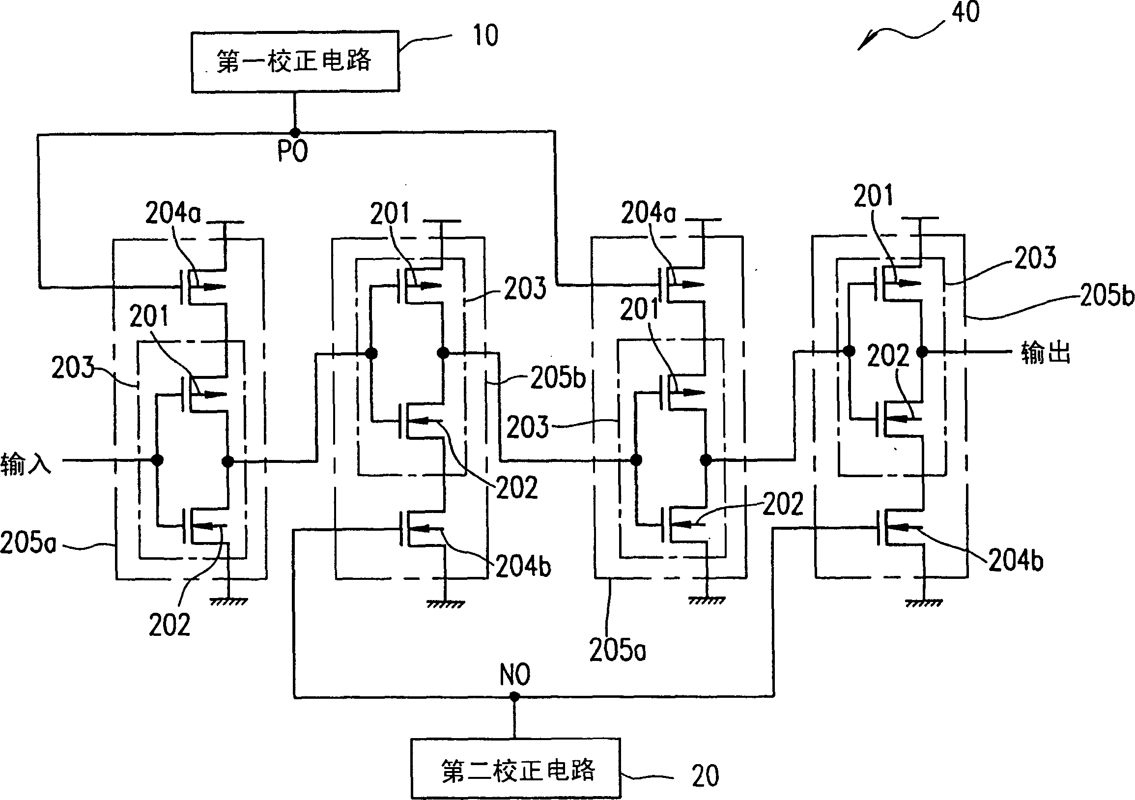
[0102] figure 1 An example delay circuit 40 according to the invention is shown. previously discussed about Figure 8 and 16 The same elements have the same reference numerals, and their detailed descriptions will be omitted below.

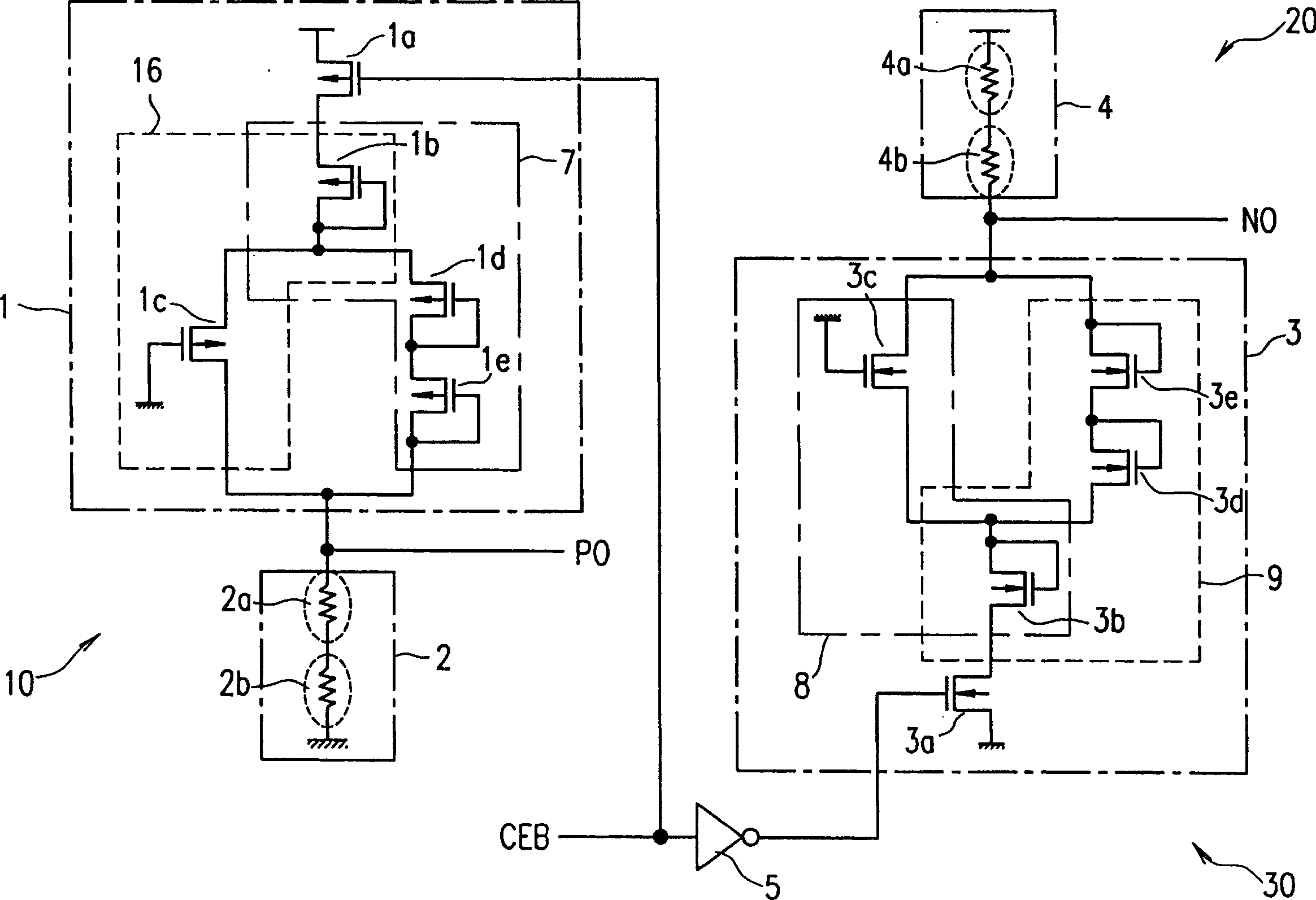
[0103] The delay circuit 40 includes a first correction circuit 10 and a second correction circuit 20, instead of Figure 8 A first correction circuit 210 and a second correction circuit 220 in the delay circuit 200 are shown. The gate of the p-channel transistor 204a included in the inverter circuit 205a receives the voltage (control signal) generated in the first correction circuit 10 . The gate of the n-channel transistor 204b included in the inverter circuit 205b receives the voltage (control signal) generated in the second correction circuit 20 . Except for these points, the delay circuit 40 has the same circuit configu...


PUM


Abstract

A correction circuit for generating a control signal for correcting a characteristic change of a first transistor includes a control signal adjusting section including a constant voltage reduction element for determining either one of a maximum voltage and a minimum voltage of the control signal and a second transistor for determining a characteristic of the control signal, a gate electrode of the second transistor receiving a prescribed voltage; and a resistor section including two types of resistor elements having resistance values of different temperature dependency characteristics from each other, the resistor elements being connected in series. The constant voltage reduction element, the second transistor, and the resistor section are connected in series between a supply terminal and a ground terminal. The control signal is output from a connection point between the control signal adjusting section and the resistor section.

Description

technical field [0001] The present invention relates to a correction circuit for use in a correction circuit for generating a control signal that corrects a change in characteristics caused by production conditions or physical conditions such as changes in power supply and temperature conditions in transistors included in semiconductor integrated circuits; And the delay circuit and the ring oscillator circuit in this correction circuit. In particular, the present invention relates to a correction circuit, a delay circuit and a ring oscillator circuit which can be preferably used to generate a reference clock generation circuit (timing generation circuit) in, for example, an internal subsynchronous semiconductor memory device. Background technique [0002] In CMOS semiconductor integrated circuits, some delay circuits used as timing generating circuits or the like use CMOS transistors. A delay circuit using a CMOS transistor utilizes the signal transmission delay characteris...

Claims


Application Information

Patent Timeline
Patent Type & Authority Applications(China)
IPC IPC(8): H03K3/011H03K3/03H03K3/354H03K5/00H03K5/13H03K19/003
CPCH03K3/0315H03K2005/00039H03K3/011H03K5/132H03K5/133H03K2005/00026H03K2005/0013H03K2005/00208H03K2005/00143
Inventor 森川佳直
Owner SHARP KK
Why Eureka
Try Eureka