Memory element and its production method

A technology for storage elements and manufacturing methods, which is applied in semiconductor/solid-state device manufacturing, electrical components, electrical solid-state devices, etc., and can solve problems such as interface breakdown

Inactive Publication Date: 2004-02-25
MACRONIX INT CO LTD
View PDF1 Cites 2 Cited by
  • Summary
  • Abstract
  • Description
  • Claims
  • Application Information

AI Technical Summary

Problems solved by technology

The buried bit line is formed in the source or drain region of the memory cell, however, a huge depletion region sometimes exists in the buried bit line region, resulting in the occurrence of punchthrough phenomenon

Method used


Image

  • Memory element and its production method
  • Memory element and its production method
  • Memory element and its production method

Examples


Embodiment Construction

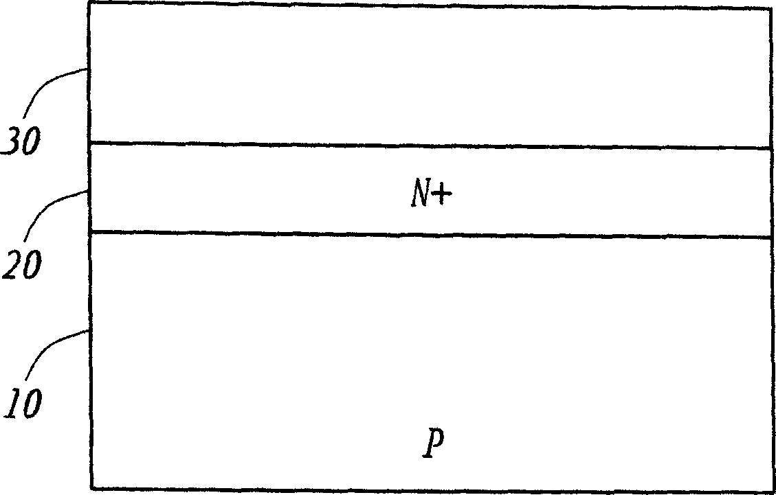
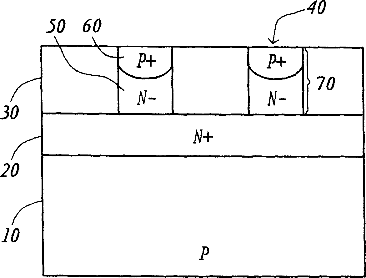
[0018] Please refer to Figure 1A ~ 1C , which shows a flowchart of a method of manufacturing a memory cell according to a preferred embodiment of the present invention. exist Figure 1A In, first, a semiconductor substrate 10 is defined, such as a p-type substrate. Next, a doped layer 20 is provided on the semiconductor substrate 10, and the doped layer 20 is used as a buried bit line of the memory cell. In one embodiment, the doped layer 20 can be doped with a large amount of n-type dopants (dopants), such as phosphorus, antimony or arsenic, and the electric energy and dose range during doping are about 35-150 keV ( kev) and 5×10 19 ~5×10 20 Atoms / square centimeter (atoms / cm 2 ), dopants can be introduced via ion implantation. After the doped layer 20 is formed, a dielectric layer 30 is deposited on the doped layer 20 with a thickness of about 200-600 nanometers (nm), and the dielectric layer 30 may be an oxide layer.

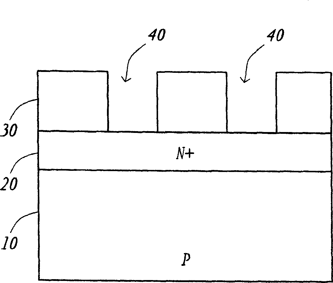
[0019] exist Figure 1B In the dielectric layer ...


PUM


Abstract

The production method of storage element includes the following steps: firstly, defining semiconductor substrate with first dopant type, providing doped layer of second dopant type on the substrate, providing dielectric layer on the doped layer, forming plug in dielectric layer, doping the dopant of second dopant type in whole area of the plug, doping the dopant of first dopant type in plug of second dopant type and providing the storage unit on the plug.

Description

technical field [0001] The present invention relates to a semiconductor circuit element and a manufacturing method, and in particular to a semiconductor memory cell and a manufacturing method. Background technique [0002] Memory cells using electrically writable and erasable phase change substances are well known technologies, such as those disclosed in US Pat. In a typical memory cell structure, diodes with buried bit lines on the X-axis or Y-axis can be used to locate and isolate individual memory cells. The buried bit line is formed in the source or drain region of the memory cell, however, sometimes a huge depletion region exists in the buried bit line region, resulting in the occurrence of punchthrough phenomenon. [0003] The interface breakdown phenomenon is a collapse phenomenon, and when the reverse bias voltage on the drain increases, the drain depletion region will expand and cause this collapse phenomenon. The electric field on the reverse biased drain will pe...

Claims


Application Information

Patent Timeline
Patent Type & Authority Applications(China)
IPC IPC(8): H01L21/768H01L21/8239H01L21/8242H01L21/8247H01L27/24H01L45/00
CPCH01L45/04H01L27/24H10B63/20H10N70/231H10N70/826
Inventor 陈旭顺庄立欣龙翔澜陈逸舟
Owner MACRONIX INT CO LTD
Why Eureka
Try Eureka