Apparatus and method for inspecting pattern defect

A defect inspection and graphics technology, applied in the direction of measuring devices, optical testing flaws/defects, image communication, etc., can solve difficult and low-cost problems

Inactive Publication Date: 2004-05-05
KOKUSA ELECTRIC CO LTD
View PDF1 Cites 21 Cited by
  • Summary
  • Abstract
  • Description
  • Claims
  • Application Information

AI Technical Summary

Problems solved by technology

However, in this adjacent comparison inspection method, in order to compare electrodes between groups, it is necessary to perform alignment with high accuracy. Therefore, it is necessary to consider the shape of the pattern and so on. In order to perform correct position alignment, an extremely high-precision position alignment device is required, and it is difficult to realize a low-cost defect inspection device.

Method used


Image

  • Apparatus and method for inspecting pattern defect
  • Apparatus and method for inspecting pattern defect
  • Apparatus and method for inspecting pattern defect

Examples


Embodiment Construction

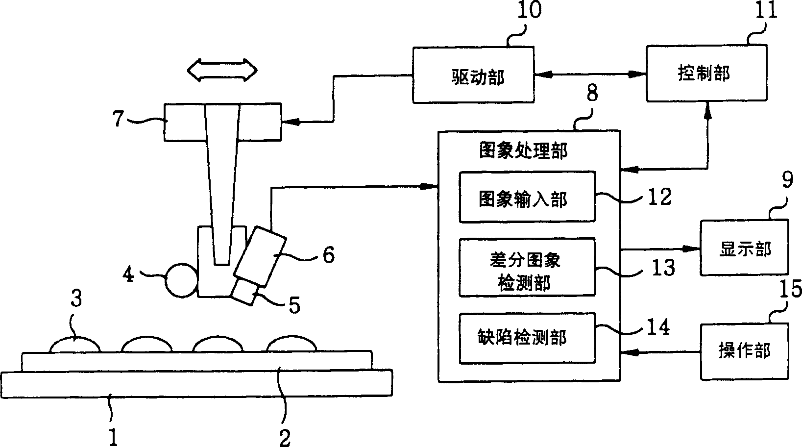
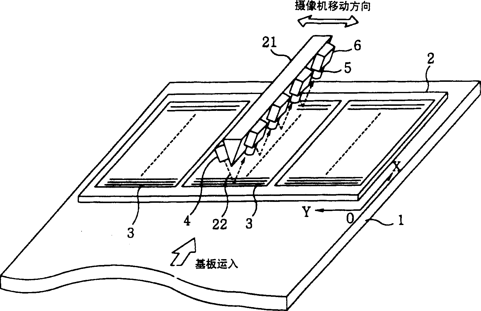
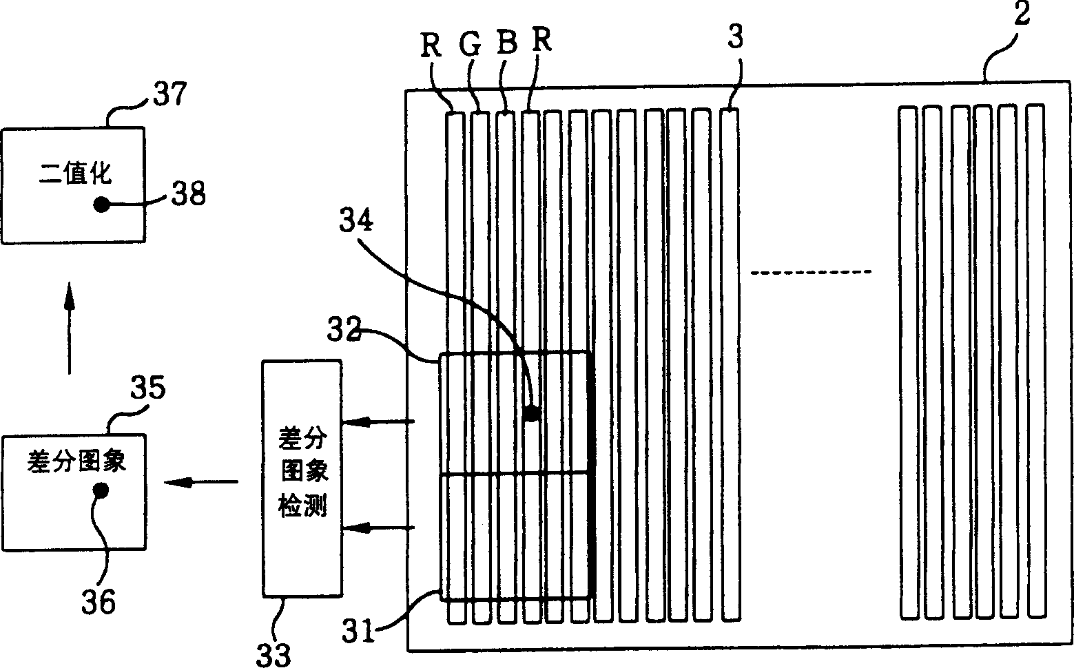
[0028] figure 1 is a diagram showing an embodiment of the pattern defect inspection device of the present invention. exist figure 1 Among them, 1 is a mounting platform for a glass substrate such as a plasma display, 2 is a glass substrate such as a plasma display, 3 is a phosphor (phosphor coating film) of R, G, and B, and 4 is for making the phosphor 3 emit light. 5 is an optical system equipped with lenses and color filters of R, G, and B, 6 is an imaging unit such as a line sensor camera for imaging, and 7 is an imaging unit 6 that makes the light source 4 The moving mechanism used to move and scan the upper surface of the glass substrate 2, 8 is an image processing part for detecting defects such as pinholes, 9 is a display part such as a color monitor or a printer for displaying inspection results or printing, and 10 is a drive A driving unit for the moving mechanism unit 7, 11 is a control unit for controlling the image processing unit 8 and the driving unit 10, and...


PUM

PropertyMeasurementUnit
widthaaaaaaaaaa

Abstract

Method and apparatus for inspecting pattern defect can inspect printing defects of fluorescent substances formed on a glass substrate such as a plasma display panel and the like automatically and rapidly without being affected by a coating pattern of the fluorescent substances, and can be installed easily in manufacturing process of the plasma display panel to thereby achieve a low cost and high speed detection. In case of inspecting the pattern defect, stripe-form pattern of the fluorescent substances formed on the glass substrate are scanned, and then a direction of the stripe-form pattern of the fluorescent substances are detected from picture signals obtained by the scanning, and then the pattern defect is inspected by comparing at least two picture data with each other, the picture data being related to the direction of the stripe-form pattern.

Description

technical field [0001] The present invention relates to a pattern defect inspection device and a pattern defect inspection method, and more particularly, to a pattern defect inspection device and a pattern defect inspection method for automatically inspecting a coating defect of a phosphor coated on a glass substrate such as a plasma display. Background technique [0002] For a pattern defect inspection device for inspecting coating or printing defects of phosphors coated or printed on a glass substrate such as a plasma display, there is a known device in the prior art. Ultraviolet rays are irradiated to a glass substrate such as a plasma display in which phosphors are formed into strips, and the formed phosphors are made to emit light. This light-emitting pattern is photographed by an imaging unit such as a line sensor (one-dimensional sensor). Since the phosphors formed are red (R), green (G), and cyan (B) phosphors, when imaging with the imaging unit, mount the correspon...

Claims


Application Information

Patent Timeline
Patent Type & Authority Applications(China)
IPC IPC(8): H01L21/66G01M11/00G01N21/64G01N21/88H01J9/42H04N17/00
CPCG01N21/95607
Inventor 渡贯明男
Owner KOKUSA ELECTRIC CO LTD
Why Eureka
Try Eureka