Multi-layer structure unit and its manufacturing method

A multi-layer structure and component technology, applied in the direction of multi-layer circuit manufacturing, printed circuit components, semiconductor/solid-state device components, etc., can solve the problem of inability to form high-precision, low-yield multilayer structure components Problems such as the fixed division of the mother board

Active Publication Date: 2004-05-19
MURATA MFG CO LTD
View PDF2 Cites 7 Cited by
  • Summary
  • Abstract
  • Description
  • Claims
  • Application Information

AI Technical Summary

Problems solved by technology

Due to the warping of the laminate, similarly to the above, there arises the problem that it is difficult to fix the mother substrate, or that it is impossible to form the conductor pattern 21 with high precision.
In addition, when dividing the mother substrate for

Method used


Image

  • Multi-layer structure unit and its manufacturing method
  • Multi-layer structure unit and its manufacturing method

Examples


Embodiment Construction

[0017] Hereinafter, embodiments of the present invention will be described with reference to the drawings.

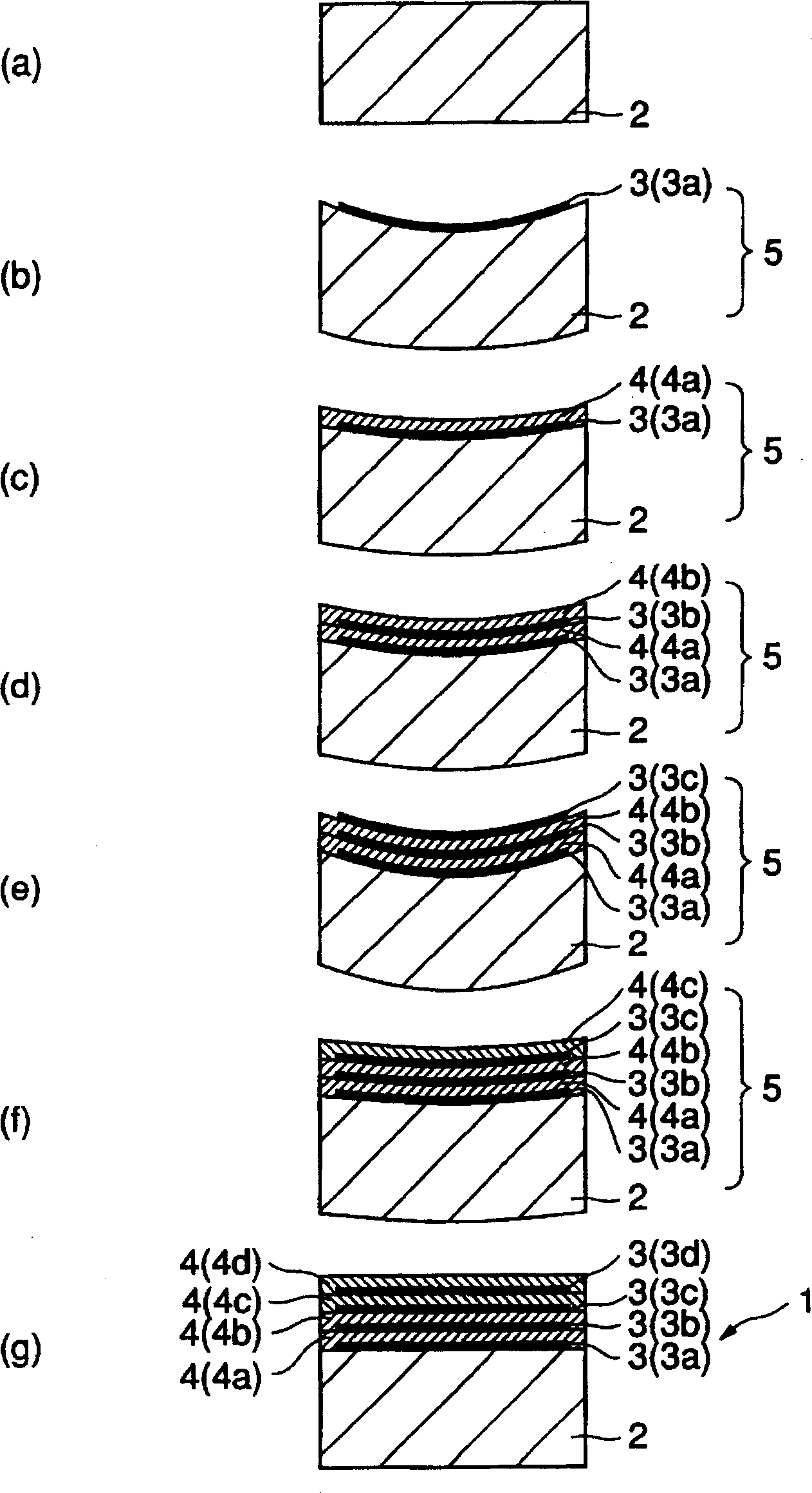
[0018] Such as figure 1 As shown in (g), the multilayer structural component 1 of this embodiment has a mode of alternately laminating the conductor pattern 3 and the insulating layer 4 on the surface side of the insulator substrate 2. The most important feature is that a plurality of insulating layers 4 ( At least one layer among 4a, 4b, 4c, and 4d) is made of an insulating material having a different thermal expansion ratio from the other insulating layers 4 .

[0019] Hereinafter, a specific configuration of the multilayer structure member 1 of this embodiment will be described together with an example of a manufacturing process. For example, first, prepare as figure 1 Insulator substrate 2 shown in (a). The insulating substrate 2 is made of, for example, an alumina substrate or a glass substrate. On the upper surface of the insulating substrate 2, a conductor ...


PUM


Abstract

The purpose of the present invention is to correct the warpage of multilayer composite 5 in the process of alternatively forming conductor pattern 3 and insulation layer 4 on the insulation body substrate 2. In the process of alternatively forming conductor pattern 3 and insulation layer 4 on the insulation body substrate 2, the constituting material of the insulation layer is modified to be the other insulation material which can correct the warpage of the multilayer composite 5 according to the predetermined schedule, or in the forming step to constitute the multilayer composite 5 by the insulation substrate 2, conductor pattern 3 and insulation layer 4. Thus, the insulation layer 4 is formed, and thereby the warpage of the multilayer composite 5 can be corrected with high accuracy.

Description

technical field [0001] The invention relates to a multi-layer structural component made by laminating conductor patterns and insulating layers on an insulating substrate and a manufacturing method thereof. Background technique [0002] As one of the electronic components, there is a multilayer structural component composed of sequentially laminating conductor patterns through insulating layers on an insulator substrate. This multilayer structural member can be produced as follows (for example, refer to Patent Documents 1 and 2). For example, if figure 2 As shown in (a), the conductor pattern 21 is formed on the insulator substrate 20 with a conductor paste or the like, and then the conductor pattern 21 is fired and the insulator pattern 21 and the conductor pattern 21 are cooled. The conductive pattern 21 shrinks during sintering, and the insulating substrate 20 and the conductive pattern 21 shrink during cooling. Since the conductor pattern 21 has a greater thermal contr...

Claims


Application Information

Patent Timeline
IPC IPC(8): H01L23/15H05K1/02H05K1/03H05K3/46
Inventor 户波与之杉山雄二伊波通明
Owner MURATA MFG CO LTD
Why Eureka
Try Eureka