Glass panel based chip type LCD device

A liquid crystal display device, chip-type technology, applied in identification devices, static indicators, optics, etc., can solve problems such as drive circuits not working properly

Active Publication Date: 2004-05-26
HYDIS TECH
View PDF0 Cites 9 Cited by
  • Summary
  • Abstract
  • Description
  • Claims
  • Application Information

AI Technical Summary

Problems solved by technology

[0008] For this reason, after several driving circuits are connected, in the driving circuit after a certain stage, the actual input driving voltage will drop to th

Method used


Image

  • Glass panel based chip type LCD device
  • Glass panel based chip type LCD device
  • Glass panel based chip type LCD device

Examples


Embodiment Construction

[0023] Hereinafter, preferred embodiments of the present invention will be described in more detail with reference to the accompanying drawings. In order to maintain the consistency of description, the same reference symbols are used in the drawings to indicate the same or similar structural elements and signals.

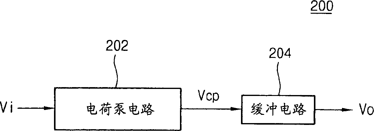
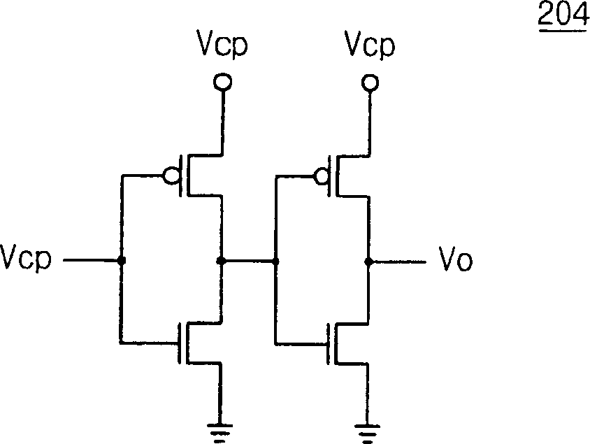
[0024] figure 2 is a block diagram of a driving voltage generating section according to an embodiment of the present invention. Such as figure 2 As shown, each driver IC has a driving voltage generating unit 200 composed of a charge pump circuit 202 and a buffer circuit 204 .

[0025] The charge pump circuit 202 boosts the driving voltage (Vi) applied from the front-end driver IC to a predetermined level and outputs a voltage (Vcp). The charge pump circuit 202 is well known in the industry, so its specific structure will not be described here. The buffer circuit 204 stabilizes the voltage (Vcp) output from the charge pump circuit 202 to generate a voltage (Vo)...


PUM


Abstract

Disclosed is a chip-on-glass type liquid crystal display (LCD). The LCD is directed to provide a construction in a way that, while each wiring for supplying driver circuits with a driving voltage is directly formed on an LCD panel through application of COG (Chip-On-Glass) technology for producing TFT-LCD, even though the wirings are connected in series between the driver circuits, the driving voltage capable of normally operating the driver circuits is supplied to all driver circuits. To this end, in consideration of a voltage drop at the panel wiring, by increasing and outputting a driving voltage, the driving voltage inputted into an n driver circuit is made to be equal to the driving voltage inputted into an (n+1) driver circuit. To accomplish this object, a driving voltage generating section is provided to each driver IC, and comprises a charge pumping circuit for increasing the leading gate driving voltage to a predetermined level, and a buffer circuit for stabilizing an output voltage of the charge pumping circuit.

Description

technical field [0001] The present invention relates to a liquid crystal display device, in particular to a chip-on-glass liquid crystal display device in which wiring between drive circuits is directly formed on a liquid crystal screen. Background technique [0002] The active matrix type liquid crystal display device has thin film transistors (thin film transistors: hereinafter referred to as “TFT”) disposed near intersections of a plurality of scanning lines and a plurality of signal lines, and liquid crystal pixels are driven by the TFTs. The scan lines are connected to an external gate driver IC that supplies scan signals. The signal lines are connected to an external source driver IC that supplies image signals. Through the TFT turned on by the scan signal, the image signal input from the source driver IC is supplied to the liquid crystal to display the specified image. [0003] In the method of connecting the scanning line to the gate driver IC and the signal line t...

Claims


Application Information

Patent Timeline
IPC IPC(8): G02F1/1345G02F1/133G09F9/00G09G3/20G09G3/36
CPCG09G3/3611G09G2320/0223G09G3/3648G02F1/133
Inventor 郑京薰成乐铉
Owner HYDIS TECH
Why Eureka
Try Eureka