Integrated circuit packaging body

A technology for integrated circuits and packages, applied in the field of integrated circuit packages, can solve problems such as the inability to effectively reduce the size, the length of the gold wire, and the reduction in the proper rate of wire bonding.

Inactive Publication Date: 2004-07-28
林宜静
View PDF0 Cites 0 Cited by
  • Summary
  • Abstract
  • Description
  • Claims
  • Application Information

AI Technical Summary

Problems solved by technology

In this way, the length of the gold wire 98 required for wire bonding is longer, and the proper rate of wire bonding will also be reduced accordingly.
What's more, the size of the package body 90 will not be effectively reduced

Method used


Image

  • Integrated circuit packaging body
  • Integrated circuit packaging body
  • Integrated circuit packaging body

Examples


Embodiment Construction

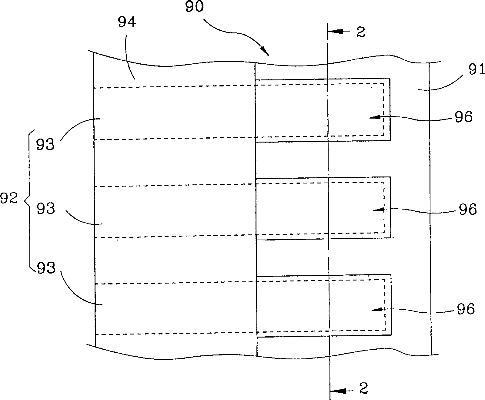
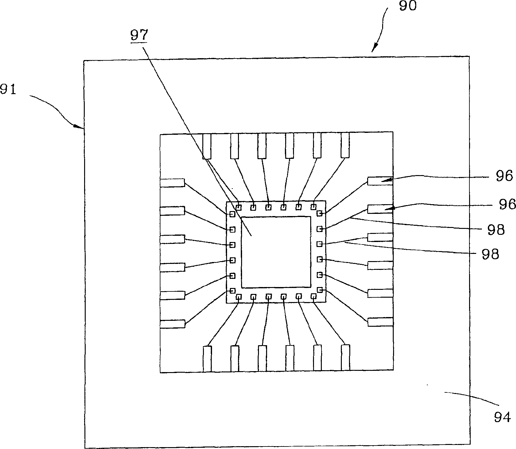
[0032] see Figure 5 As shown in FIG. 8, the structure of the integrated circuit package 1 provided by the first preferred embodiment of the present invention mainly includes a substrate 10 and a circuit layout 20, which are composed of a plurality of copper wires 21, which can be arranged on one or both sides of the substrate 10 . A solder resist layer 30 is disposed on the substrate 10 to cover a predetermined portion of the circuit layout 20 and a plurality of conductors 40 .

[0033] For making the integrated circuit package 1 of the present invention, please refer to Figure 5 As shown, firstly, the substrate 10 is prefabricated with the circuit layout 20 and the solder resist layer 30 thereon. The circuit layout 20 defines a plurality of connecting portions 22 .

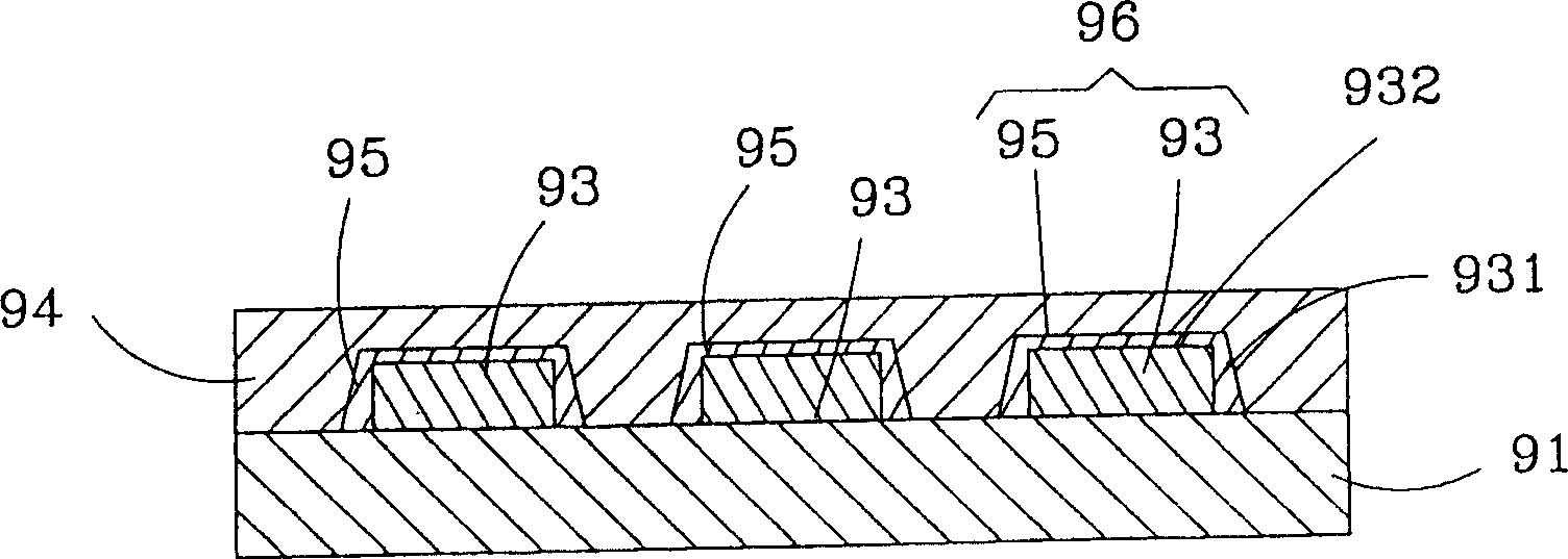
[0034] Next, if Image 6 As shown, using the existing photo-chemical method (photo-chemical method), the part of the solder resist layer 30 above the conductive part 22 corresponding to the circuit layout 2...


PUM


Abstract

The invention relates to an IC packaging body to load at least an electronic component (wafer), containing: a circuit layout composed of plural lead wires and having plural connector parts; a soldering-resistant layer covering the preset part of the circuit layout and formed with equal-microholes; and plural connector bodies in these equal microholes, clinging to and connected with the conductive parts, respectively. Therefore, the circuit layout can be connected together by the equal connector bodies and the electronic component (wafer).

Description

technical field [0001] The present invention is related to electronic products, in particular to an integrated circuit packaging body. Background technique [0002] figure 1 and figure 2 An existing IC package carrier (IC package carrier) 90 is shown, which includes a substrate (substrate) 91, one or both sides of which have a circuit layout (conductor pattern) composed of a plurality of copper traces (copper traces) 93 92 , and the circuit layout 92 is covered with a solder mask 94 . Usually a predetermined portion of the solder resist layer 94 will be removed, so that the predetermined portion of the wire 93 of the circuit layout 92 is exposed, and then nickel and gold plating 95 is plated on the surface of the exposed wire 93, so that, That is, pads 96 forming the circuit layout. [0003] When the integrated circuit package 90 is electrically connected to a die 97 by wire bonding, please refer to image 3 As shown in FIG. 4 , gold wires 98 can be used to connect the...

Claims


Application Information

Patent Timeline
IPC IPC(8): H01L23/12H01L23/50
CPCH01L2924/0002H01L2224/48091H01L2224/49171
Inventor 林宜静
Owner 林宜静
Why Eureka
Try Eureka