Probe, probe assembly method and probe plate

A technology of probes and positioning devices, which is applied in the field of probe boards, can solve the problems of limited movement of contact probes, difficulty in adjusting the position and posture of contact probes freely and in all directions, and achieve the effect of reducing the number of probes

Inactive Publication Date: 2004-08-25
YAMAICHI ELECTRONICS
View PDF0 Cites 8 Cited by
  • Summary
  • Abstract
  • Description
  • Claims
  • Application Information

AI Technical Summary

Problems solved by technology

Since the resin film is difficult to bend along the surface of the film, the direction in which the contact probe can move relative to the printed circuit board is limited
Therefore, for the probes disclosed in patent documents #1, #2, and #3, it is difficult to freely and omnidirectionally adjust the position and posture of each contact probe

Method used


Image

  • Probe, probe assembly method and probe plate
  • Probe, probe assembly method and probe plate
  • Probe, probe assembly method and probe plate

Examples


Embodiment Construction

[0044] Embodiments of the present invention will be described in detail below with reference to the accompanying drawings.

[0045] (The overall structure of the probe card)

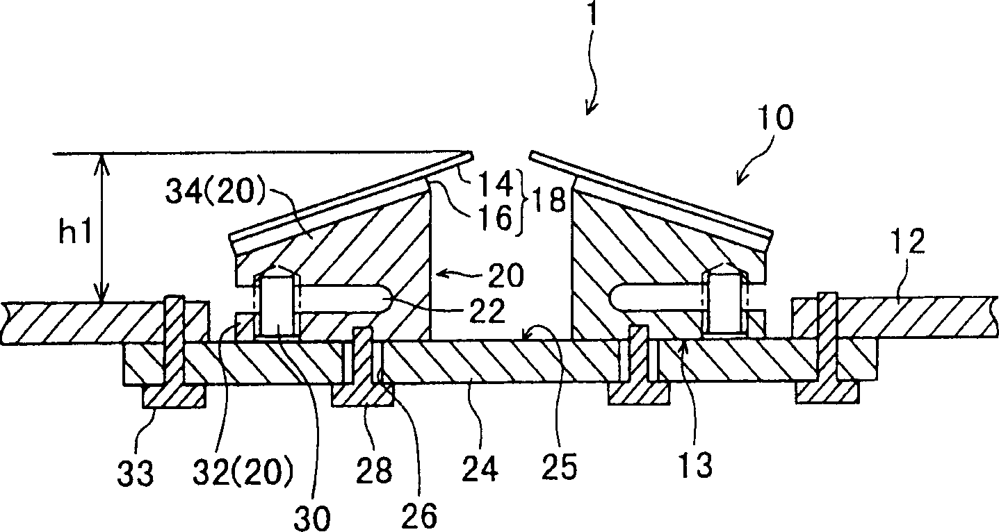
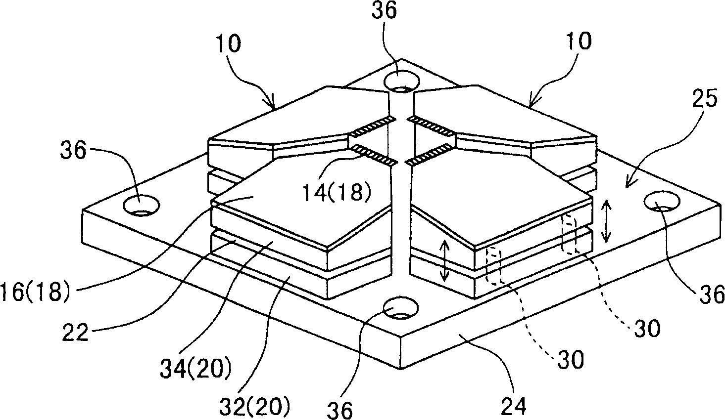
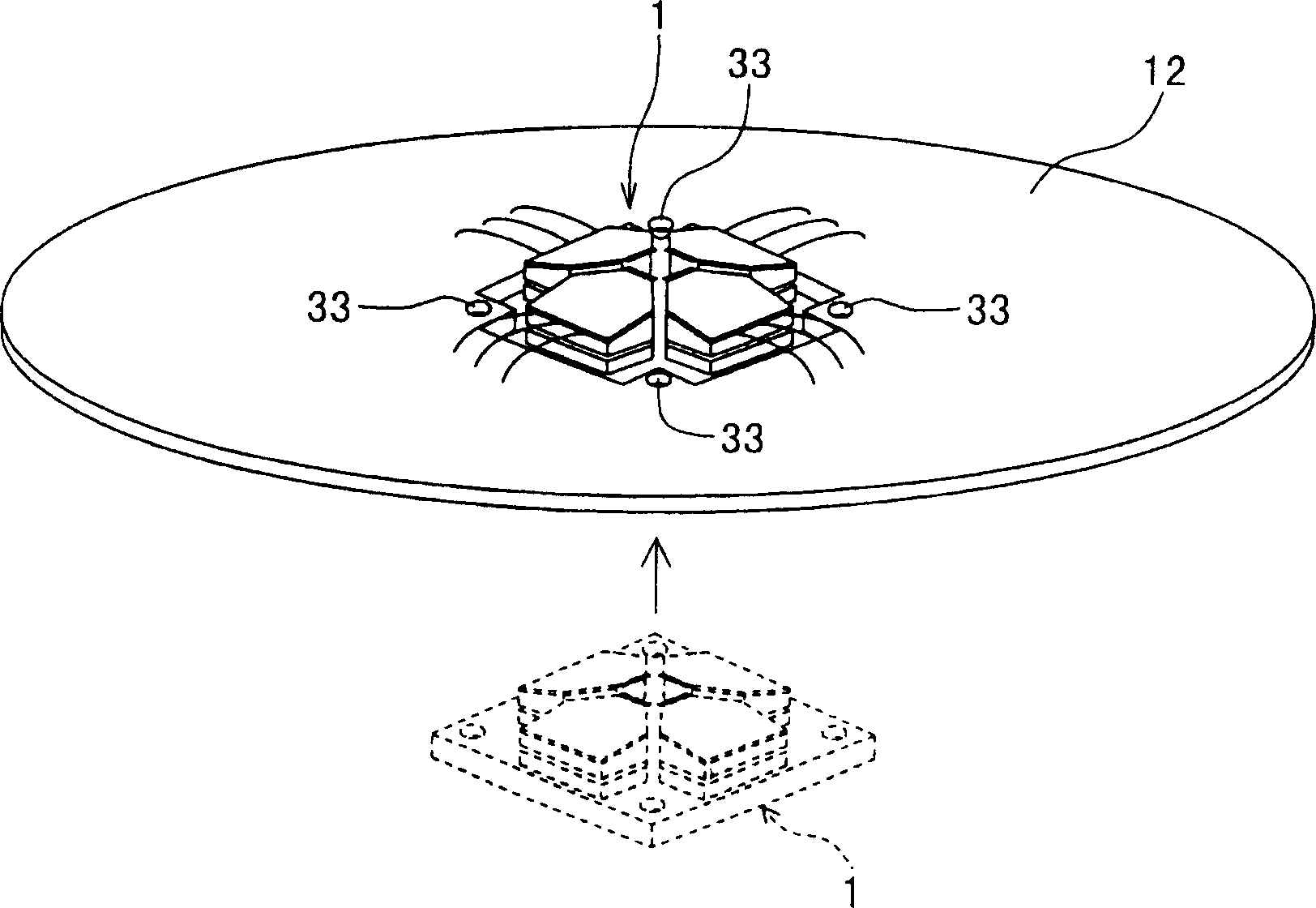
[0046] figure 1 is the cross-sectional view of the probe card; figure 2 is a perspective view of probe 1 of the probe card; image 3 is a perspective view of a probe card according to an embodiment of the present invention. The probe card is mounted on a detection device (probe) for detecting electrical characteristics of electronic devices such as semiconductor integrated circuits and liquid crystal panels. This probe card has a plurality of probes 14 that are in contact with electrodes of the electronic device. The probe 1 is fixed to the printed circuit board 12 with screws 33 . The printed circuit board 12 electrically connects the detection circuit of the detector main system and the probe 14 . A spacer (not shown) may be inserted between the probe 1 and the printed circuit board 12 to adjust...


PUM


Abstract

Probe head, its assembly method and probe card. A slide unit is slid on a flat slide plane of a table to adjust the relative positions of a plurality of slide units along a direction parallel to the flat slide plane. Even if the slide unit moves together with a movable unit along the direction parallel to the flat slide plane, the relative positions of a plurality of movable units will not change along a direction vertical to the flat slide plane. By sliding the slide unit on the flat slide plane of the table and moving the movable unit along the direction vertical to a slide surface, the relative positions of a plurality of probes mounted on the movable units can be adjusted independently and separately along the directions parallel to and vertical to the flat slide plane.

Description

technical field [0001] The present invention relates to a probe for testing electrical characteristics of electronic devices such as semiconductor integrated circuits and liquid crystal panels, a method of assembling the probe, and a probe card. In the embodiment of the present invention, it is considered that the probe card has a printed circuit board mounted on a detection device (probe) and a probe fixed to the printed circuit board, and the probe has a plurality of probes (probe pins) . Background technique [0002] In a conventional method of inspecting electrical characteristics of an electronic device, a probe card provided with a plurality of probes having protruding tips is lowered so as to bring the tips of the probes into contact with electrodes of the device. As the integration level of electronic devices continues to increase, the distance between electrodes becomes smaller and smaller. Therefore, it is more necessary to perform an alignment operation between ...

Claims


Application Information

Patent Timeline
Patent Type & Authority Applications(China)
IPC IPC(8): G01R1/06G01R1/073G01R31/28H01L21/66
CPCG01R31/2887H01L2224/48091H01L2924/00014A23C11/103A23C20/025A47J27/00A47J36/00A23L11/07
Inventor 泽田修一土江雅也
Owner YAMAICHI ELECTRONICS
Why Eureka
Try Eureka