

Method and equipment for manufacturing semiconductor devices
A manufacturing method and semiconductor technology, applied in the direction of semiconductor/solid-state device manufacturing, electrical components, circuits, etc., can solve the problems of damage flexural strength, chip surface pollution, distortion, etc., and achieve the effect of preventing cracking and inhibiting the reduction of flexural strength.
- Summary
- Abstract
- Description
- Claims
- Application Information
AI Technical Summary
Problems solved by technology
Method used
Image

Examples
no. 1 Embodiment
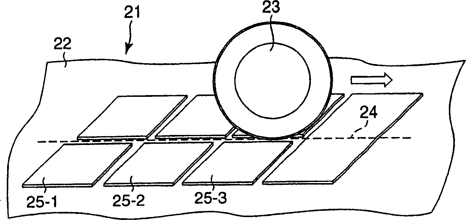
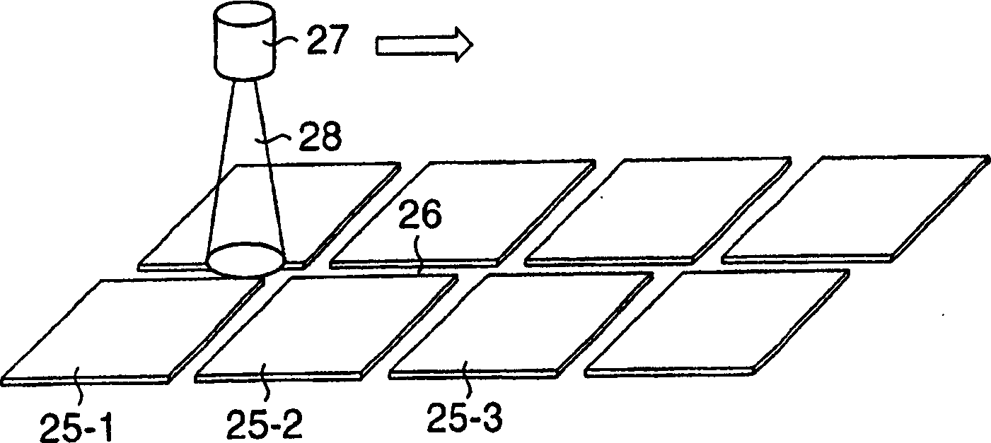
[0038] figure 1 with figure 2are diagrams for explaining the semiconductor device manufacturing method and the semiconductor device manufacturing equipment according to the first embodiment of the present invention, respectively, figure 1 Indicates the scribing process, figure 2 It shows the process of scribe area processing by irradiating a laser beam to a scribe area.
[0039] First, various semiconductor elements are formed in a semiconductor wafer according to well-known manufacturing processes.
[0040] Next, an adhesive sheet 22 is attached to the back surface of the element formation surface of the semiconductor wafer 21 on which the above-mentioned elements have been formed by means of a sheet adhesive device, and the adhesive sheet 22 is adsorbed and fixed on a dicing table. And, from the main surface side of the semiconductor wafer 21, use a dicing machine (such as a diamond knife 23), perform dicing along the scribing line 24, and separate them into individua...
no. 2 Embodiment
[0049] In the first embodiment described above, the case where the semiconductor wafer 21 is fully cut during dicing has been described as an example. However, it can also be similarly applied to a manufacturing process in which the semiconductor wafer 21 is cut in half to form grooves, and the back surface is ground and divided (pre-scribing method).
[0050] That is, according to well-known manufacturing processes, after forming various semiconductor devices on a semiconductor wafer, the semiconductor wafer 21 is diced from the main surface side along dicing lines or chip dividing lines to form half dicing grooves. In order to form the half-cut groove, for example, use such as figure 1 A diamond knife 23 as shown. The depth of the notch is only about 10-30 μm (at least 5 μm) deeper than the final processing thickness of the chip. How much depends on the precision of the dicing machine and the grinding machine.
[0051] Then, if figure 2 As shown, the laser beam 28 is i...
Deformed example 1
[0065] By installing a treatment tank for storing semiconductor wafers in water and irradiating laser beams in the water, temperature control will be facilitated, and the increase in chip temperature caused by laser beam irradiation can be suppressed.
PUM
 Abstract
Description
Claims
Application Information