Semiconductor device, electronic apparatus and their manufacturing methods, electronic equipment

A technology of electronic equipment and manufacturing method, which is applied in the direction of semiconductor/solid-state device manufacturing, semiconductor devices, semiconductor/solid-state device components, etc., and can solve problems such as unstable installation state, non-uniform component size, and difficulty in stacking different types of chips

Inactive Publication Date: 2004-09-22
SEIKO EPSON CORP
View PDF0 Cites 2 Cited by
  • Summary
  • Abstract
  • Description
  • Claims
  • Application Information

AI Technical Summary

Problems solved by technology

[0003] However, in the method of three-dimensionally mounting semiconductor chips while inserting the same type of carrier substrate, it becomes difficult to stack different types of devices, and it becomes difficult

Method used


Image

  • Semiconductor device, electronic apparatus and their manufacturing methods, electronic equipment
  • Semiconductor device, electronic apparatus and their manufacturing methods, electronic equipment
  • Semiconductor device, electronic apparatus and their manufacturing methods, electronic equipment

Examples


Embodiment Construction

[0041] Next, a semiconductor device, an electronic device, and a manufacturing method thereof according to embodiments of the present invention will be described with reference to the drawings.

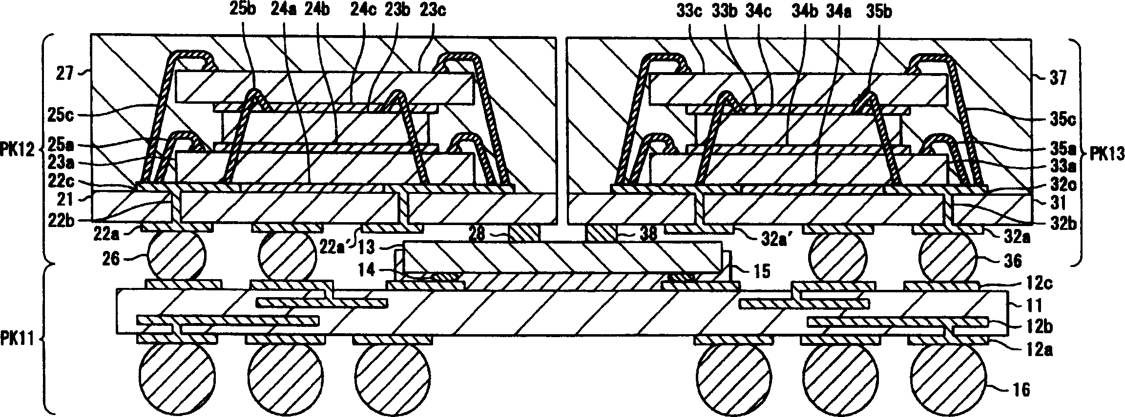
[0042] figure 1 is a cross-sectional view showing the structure of the semiconductor device according to Embodiment 1, figure 2 is a plan view showing a schematic configuration of the semiconductor device according to Embodiment 1. In the first embodiment, semiconductor packages PK12 in which semiconductor chips (or semiconductor stampers) 23a to 23c in a stacked structure are connected by wire bonding are stacked on semiconductor package PK11 in which semiconductor chips (or semiconductor stampers) 13 are mounted by ACF bonding. The semiconductor package PK13 of the stacked semiconductor chips (or semiconductor stampers) 33a-33c is connected by wire bonding.

[0043] figure 1 In the semiconductor package PK11, a carrier substrate 11 is provided, and lands (1 and 12c) are formed o...


PUM


Abstract

A technique is provided to three-dimensionally mount different types of packages with stability. According to the technique, projections are contacted to a semiconductor chip and bumps are bonded to lands disposed on a first carrier substrate so that an end of each other carrier substrate is held right above the semiconductor chip and the other carrier substrates are independently mounted above the first carrier substrate.

Description

technical field [0001] The present invention relates to a semiconductor device, an electronic device, an electronic instrument, a method for manufacturing a semiconductor device, and a method for manufacturing an electronic device, and is particularly applicable to a stacked structure of semiconductor components and the like. Background technique [0002] In conventional semiconductor devices, there is a method of three-dimensionally mounting a semiconductor chip while inserting a carrier substrate of the same type in order to save space when mounting the semiconductor chip. [0003] However, in the method of three-dimensionally mounting semiconductor chips while inserting the same type of carrier substrate, it becomes difficult to stack different types of devices, and it becomes difficult to stack different types of chips. On the other hand, if only different types of modules are stacked, since the size of the modules is not uniform, the mounting state of the different type...

Claims


Application Information

Patent Timeline
IPC IPC(8): H01L25/18H01L21/56H01L23/31H01L25/065H01L25/10H01L25/11
CPCH01L2225/1058H01L2224/73203H01L2224/45124H01L25/0657H01L2924/15331H01L23/3128H01L2225/06568H01L2924/01079H01L24/48H01L2224/73204H01L2224/48465H01L25/105H01L2924/3511H01L2225/1005H01L2224/73215H01L2224/48227H01L2224/32145H01L2924/15311H01L2225/1023H01L2924/01029H01L21/563H01L2224/45144H01L2224/16225H01L2224/73265H01L2924/01013H01L2225/06562H01L2224/32225H01L24/45H01L24/73H01L2924/00014H01L2924/181H01L2924/00H01L2924/00012H01L2224/0401
Inventor 泽本俊宏
Owner SEIKO EPSON CORP
Why Eureka
Try Eureka