

High-frequency switched circuit
A high-frequency switch and circuit technology, which is applied in the direction of electronic switches, resonant circuit adjustment, electrical components, etc., can solve the problem of not being able to use high-frequency switch circuits, achieve good high-frequency characteristics, and reduce insertion loss.
- Summary
- Abstract
- Description
- Claims
- Application Information
AI Technical Summary
Problems solved by technology
Method used
Image

Examples
no. 1 Embodiment
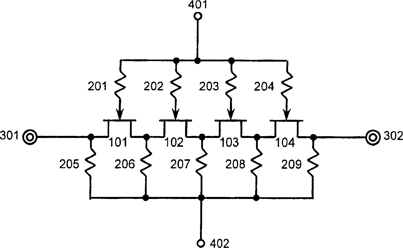
[0045] use figure 1 A circuit diagram showing a high-frequency switching circuit according to the first embodiment of the present invention. exist figure 1 In , symbols 101 to 104 denote depletion-type first to fourth FETs connected in series. Reference numerals 201 to 204 denote first to fourth resistors for applying gate bias to the first to fourth FETs 101 to 104. Reference numerals 205 to 209 denote fifth to ninth resistors for fixing source-drain voltages of the first to fourth FETs 101 to 104 . Reference numeral 301 denotes a first high-frequency signal input / output terminal, and reference numeral 302 denotes a second high-frequency signal input / output terminal. Reference numeral 401 denotes a first control terminal, and reference numeral 402 denotes a second control terminal.
[0046] Next, a specific connection relationship will be described. The drain terminal of FET101 is connected to the source terminal of FET102, the drain terminal of FET102 is connected to ...
no. 2 Embodiment
[0061] In the first embodiment of the circuit of the present invention, the resistors 205 to 209 which fix the potentials of both ends of the series circuit of FETs 101 to 104 and the intermediate connection point have a resistance value of 1 kΩ or more. The upper limit of the resistance value of the resistors 205 to 209 is not particularly specified, but practically, it is preferable to use a resistor of 1 MΩ or less to 10 MΩ or less. In addition, the resistance values of the resistors 201 to 204 are set within a range of several tens of kΩ to several hundreds of kΩ, for example.
[0062] With this structure, it is possible to prevent the signals passing through the FETs 101-104 from leaking through the resistors 205-209. Other effects are the same as those of the first embodiment.
no. 3 Embodiment
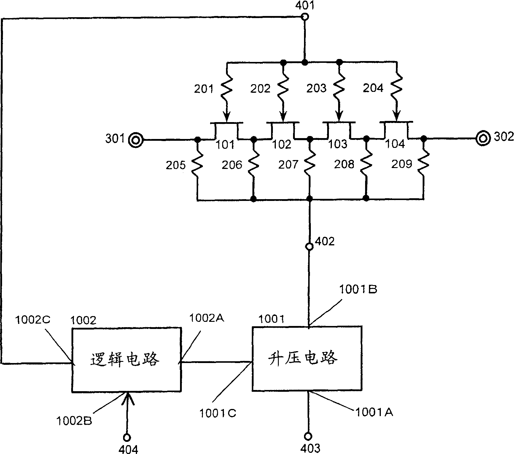
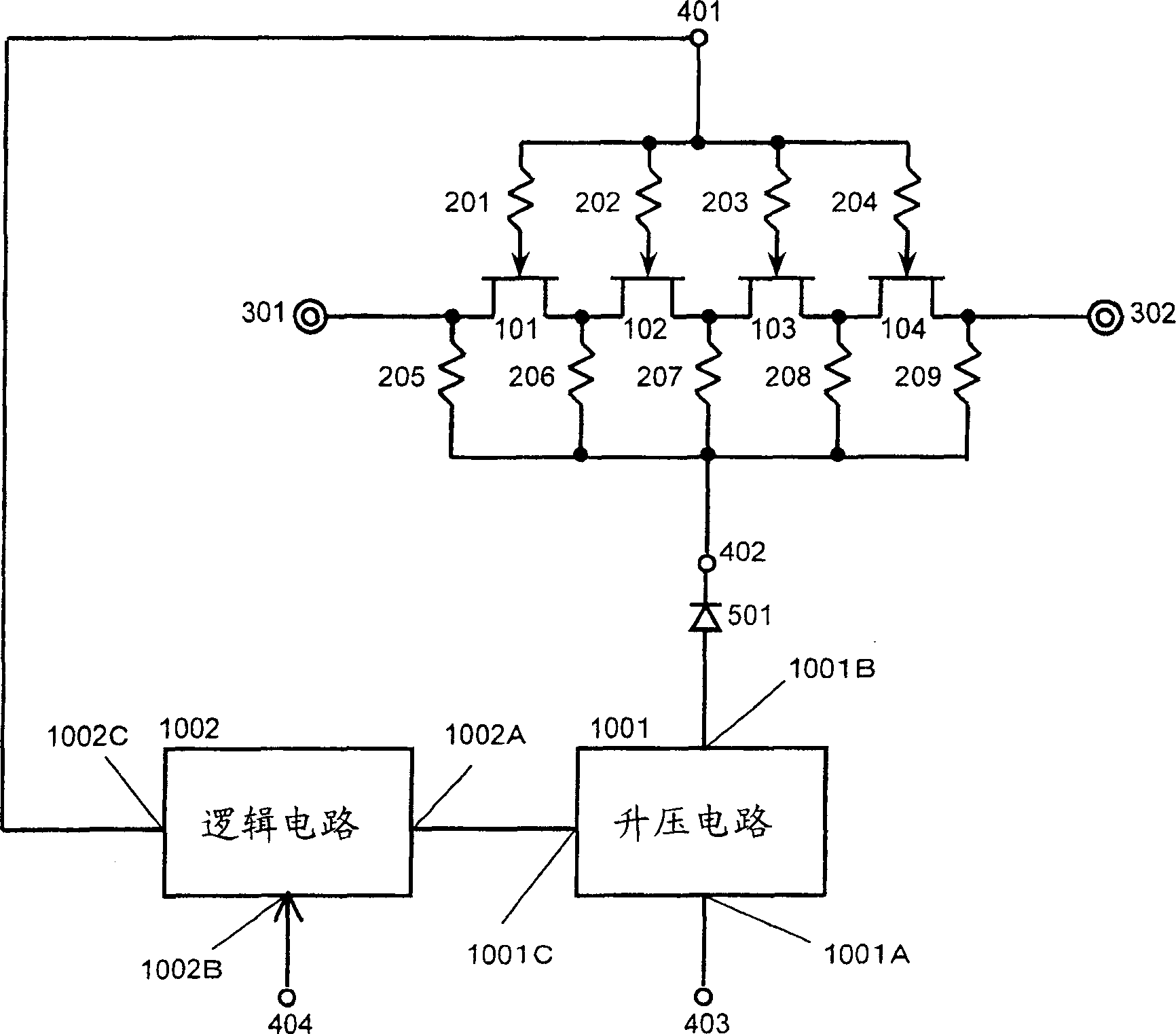
[0064] use figure 2 A circuit diagram showing a high-frequency switching circuit according to a third embodiment of the present invention. In the first embodiment described above, the voltage supplied from the outside is directly applied to the control terminal 401 and the control terminal 402 . However, the third embodiment is characterized in that the applied voltage is temporarily boosted, and the boosted voltage is applied to the control terminal 401 and the control terminal 402 .
[0065] For this reason, in the third embodiment, a booster circuit 1001 and a logic circuit 1002 are added to the structure of the first embodiment, and a control terminal 403 for applying a control voltage to the booster circuit 1001 and a control terminal 403 for the logic circuit are added. 1002 plus the control terminal 404 of the control voltage. The boost circuit 1001 boosts the voltage supplied from the control terminal 403 to a desired voltage using a charge pump. The logic circuit ...
PUM
 Abstract
Description
Claims
Application Information