Electro-optical panel driving circuit, electro-optical device provided with electro-optical panel and driving circuit, and electronic apparatus provided with electro-optical device
A panel drive circuit, electro-optic technology, applied in the direction of optics, nonlinear optics, color TV with bandwidth compression, etc., can solve the problem that the dummy circuit cannot correctly reflect the characteristics of the sampling circuit and buffer circuit, high precision, and it is difficult to fully remove the bad delay Impact and other issues
- Summary
- Abstract
- Description
- Claims
- Application Information
AI Technical Summary
Problems solved by technology
Method used
Image

Examples
no. 1 Embodiment
[0053] refer to Figure 1 to Figure 5 , to describe the first embodiment of the electro-optical device of the present invention.
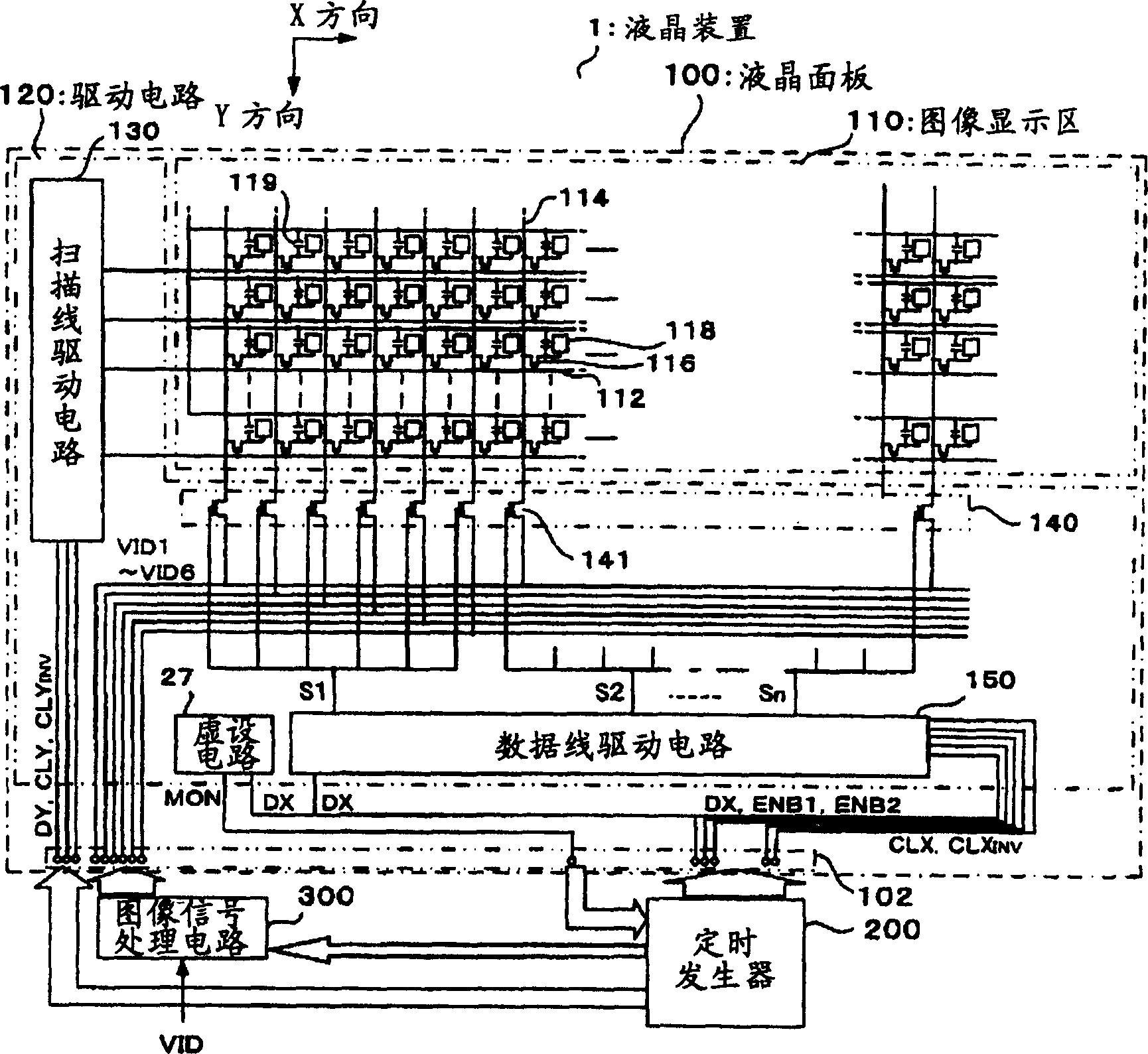
[0054] First, refer to figure 1 The overall configuration of the electro-optical device of the present invention will be described. here, figure 1 It is a block diagram showing the overall configuration of the liquid crystal device of this embodiment.
[0055] like figure 1 As shown, the liquid crystal device includes a liquid crystal panel 100 , a timing generator 200 , and an image signal processing circuit 300 as an example of the "electro-optic panel" of the present invention as main parts.
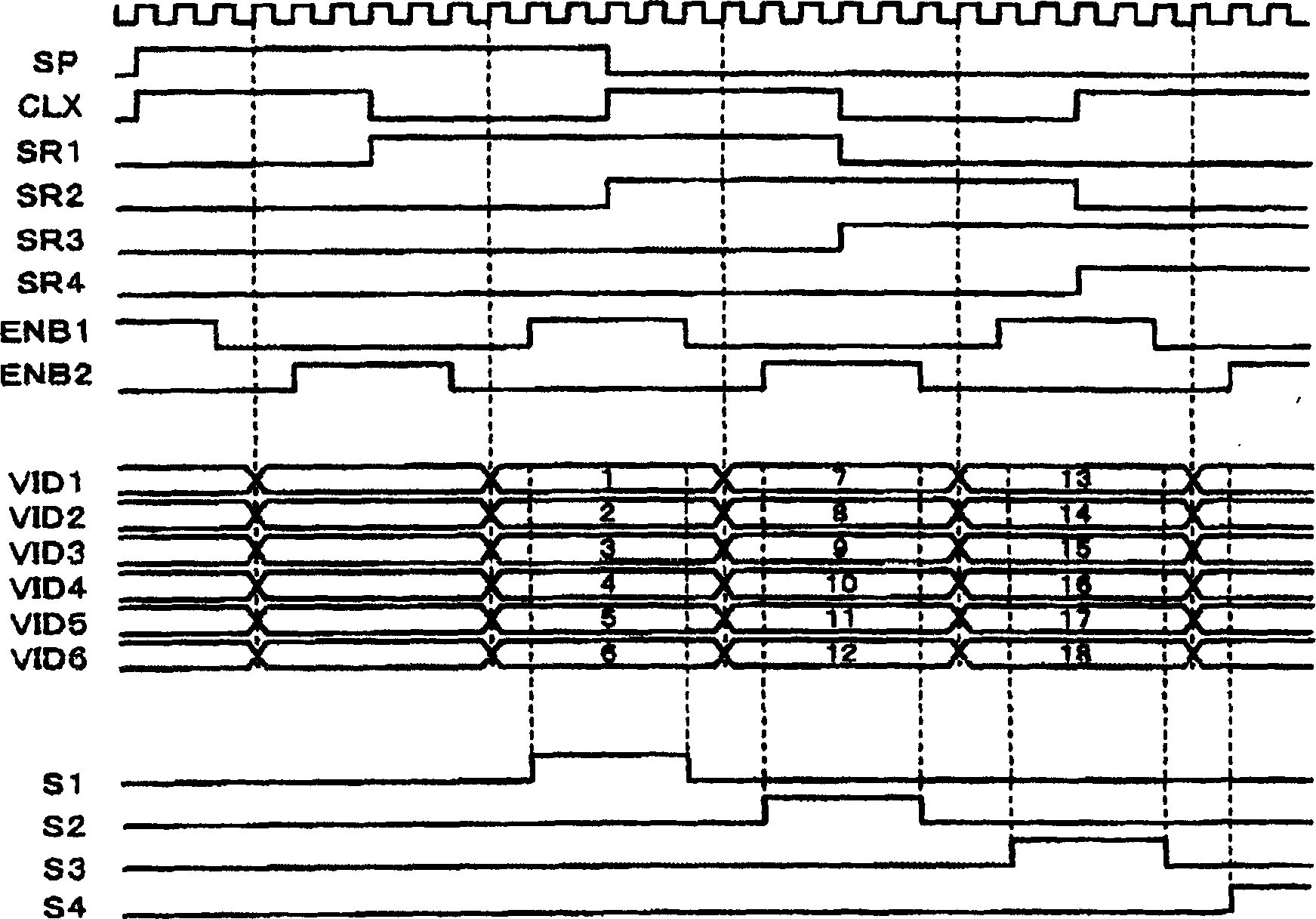
[0056] In the liquid crystal panel 100, the element substrate on which the TFT 116 is formed as a switching element and the counter substrate are opposed to the electrode formation surface, and are pasted together with a certain gap, and the liquid crystal is sandwiched in the gap. The timing generator 200 outputs various timing signals used in each p...
no. 2 Embodiment
[0102] A second embodiment of the electro-optic device of the present invention will be described below.
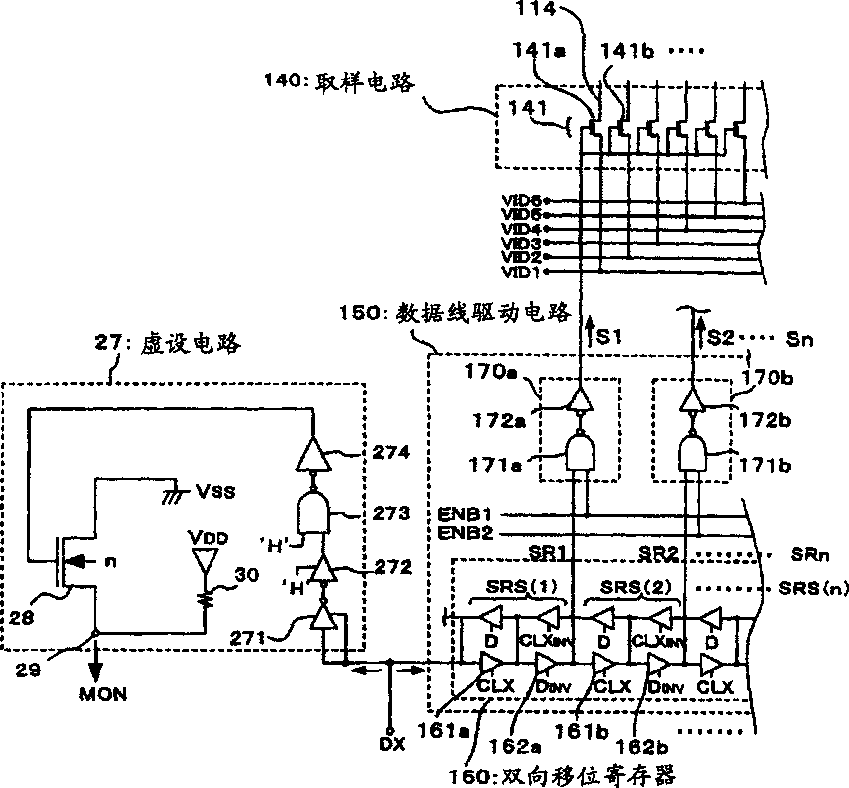
[0103] Compared with the above-mentioned first embodiment, the second embodiment is different in the size or plane figure of each constituent element of the dummy circuit 27. As for the circuit structure and operation of the dummy circuit 27, the overall structure of the liquid crystal device, and the circuits in the liquid crystal panel 100 The structure and operation are the same as those of the first embodiment. Therefore, the structure different from that of the first embodiment will be described below. In addition, since there is a one-to-one correspondence with all the constituent elements of the above-mentioned first embodiment, drawing illustration is omitted.
[0104] First, as mentioned above, in the sampling circuit 140, since a plurality of sampling switches 141 are connected in parallel, the dummy circuit 27 is also similarly connected in parallel with the s...
no. 3 Embodiment
[0113] refer to Figure 7 A third embodiment of the electro-optical device of the present invention will be described.
[0114] Compared with the above-mentioned first embodiment, the third embodiment is different in the structures of the enabling circuits 170a, 170b, . . . The overall structure and operation of the liquid crystal device are the same as those of the first embodiment. Therefore, only the configurations different from those of the first embodiment will be described.
[0115] In this example, if Figure 7 As shown, the enable circuits 170a, 170b, . That is, the configuration in the first embodiment is further configured by adding inverters 173a, 174a and the like.
[0116] According to this configuration, it is possible to suppress a large signal delay due to wiring capacitance and the like in all paths from the bidirectional shift register 160 to the sampling circuit.
[0117] At this time, even in the dummy circuit 27 which simulates the delay of the detec...
PUM
 Abstract
Description
Claims
Application Information
 - R&D
- Intellectual Property
- Life Sciences
- Materials
- Tech Scout
- Unparalleled Data Quality
- Higher Quality Content
- 60% Fewer Hallucinations
Browse by: Latest US Patents, China's latest patents, Technical Efficacy Thesaurus, Application Domain, Technology Topic, Popular Technical Reports.
© 2025 PatSnap. All rights reserved.Legal|Privacy policy|Modern Slavery Act Transparency Statement|Sitemap|About US| Contact US: help@patsnap.com