Supercharge Your Innovation With Domain-Expert AI Agents!

Electrophoretic active matrix display device

A technology for devices and driving circuits, used in static indicators, instruments, nonlinear optics, etc.

Inactive Publication Date: 2004-12-15
KONINKLIJKE PHILIPS ELECTRONICS NV
View PDF2 Cites 2 Cited by
  • Summary
  • Abstract
  • Description
  • Claims
  • Application Information

AI Technical Summary

Problems solved by technology

[0003] The drawback of this device is that the switching characteristics of the pixels should be the same throughout the device, while also requiring the long-term stability of the pixels

Method used


Image

  • Electrophoretic active matrix display device
  • Electrophoretic active matrix display device
  • Electrophoretic active matrix display device

Examples


Embodiment Construction

[0021] The scope of protection of the present invention is not limited to the embodiments described below, which relate to a switched mirror device with a hydride-based switchable material. For example, it can be applied to electrochromic devices in which the optical switching layer causes a change in the concentration of hydrogen, lithium, or oxygen ions, and in these devices, the switching threshold voltage and the degradation threshold voltage for switching the device are also relatively close to each other. Electrochromic devices constitute a family of materials in which the chemical and / or electronic state of a switchable layer is changed by reversible reduction / oxidation or another electrochemical reaction. Switched mirror devices form a family in which the chemical composition of the switchable layer changes from one hydride form to another.

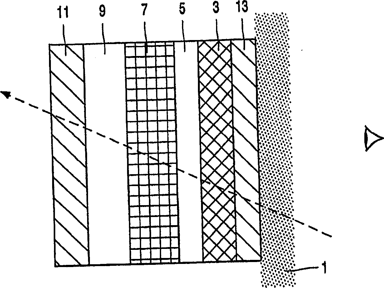
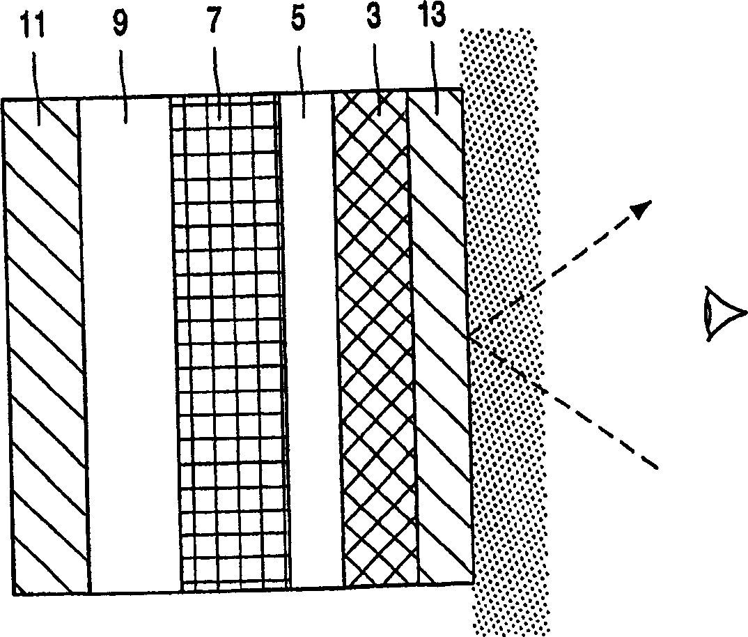
[0022] Figure 1A , 1B is the cross-sectional view of the switched mirror device. The device may be, for example, a display de...


PUM

PropertyMeasurementUnit
thicknessaaaaaaaaaa
thicknessaaaaaaaaaa
thicknessaaaaaaaaaa

Abstract

A matrix display (20) comprises pixels based on switching elements (30) which comprise a switchable layer which can be switched from one chemical state to another, the optical properties of said chemical states being different. Voltage-limiting devices (41, 42) preventing pixel degradation are arranged on the switching elements (30).

Description

technical field [0001] The present invention relates to a device comprising an array of pixels reversibly switchable between at least first and second chemical states having different optical properties, said pixels comprising a stack , the stack includes a switchable layer of optically switchable material that causes switching of the pixel from a first state to a second state. The device of the present invention also includes a driver circuit for switching said pixels. Background technique [0002] US 5,905,590 describes a switching device comprising a switching film containing hydrides of magnesium and other trivalent metals. By exchange of hydrogen, the switching film can be reversibly switched from a first transparent chemical state via an intermediate black absorbing state to a second mirror-like (perfectly reflective or scattering) chemical state with zero transmission. The switching film comprises a stack of layers deposited on a transparent substrate. Due to the o...

Claims


Application Information

Patent Timeline
Patent Type & Authority Applications(China)
IPC IPC(8): G02F1/15G02F1/163G09G3/20G09G3/34G09G3/38
CPCG02F1/163G09G2300/0842G09G3/34G09G2300/0809G09G2300/0823G09G2310/06G09G2330/04G09G2300/088G09G2320/04G09G3/38G02F1/133
Inventor P·范德斯卢斯M·T·约翰逊A·M·詹纳A·塞佩尔
Owner KONINKLIJKE PHILIPS ELECTRONICS NV
Features
  • R&D
  • Intellectual Property
  • Life Sciences
  • Materials
  • Tech Scout
  • Unparalleled Data Quality
  • Higher Quality Content
  • 60% Fewer Hallucinations
Learn More