Liquid crystal display device and electronic apparatus
A technology of liquid crystal display device and liquid crystal layer, which is applied in optics, instruments, nonlinear optics, etc., can solve the problems of insufficient display of optical anisotropic elements, high cost, and large-scale device.
- Summary
- Abstract
- Description
- Claims
- Application Information
AI Technical Summary
Problems solved by technology
Method used
Image
Examples
no. 1 Embodiment approach
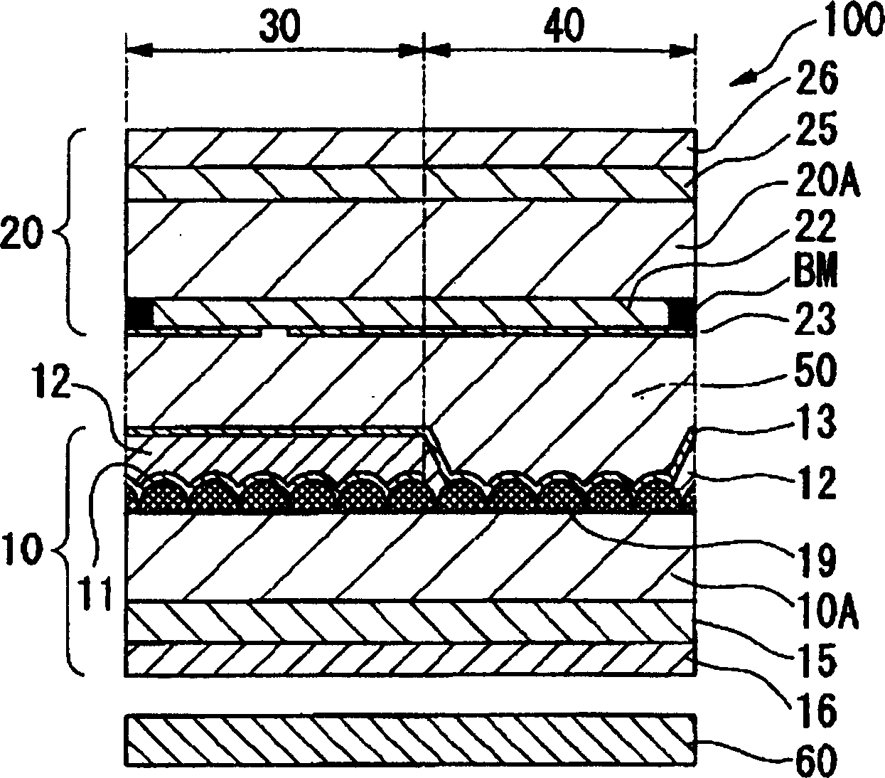
[0033] figure 1 It is an enlarged partial cross-sectional view showing a pixel portion of a liquid crystal display device having the structure of the present invention. The liquid crystal display device 100 shown in this figure is an active matrix transflective liquid crystal display device. The outer surface of 10 is provided with a backlight 60 . In addition, a reflective display region 30 and a transmissive display region 40 are provided in one pixel. In the liquid crystal display device 100 of the present embodiment, the upper side shown in the figure (the outer side of the counter substrate 20 ) is used as the display surface, and the observer who visually views the display is positioned above the figure.
[0034] exist figure 1In the array substrate 10 shown, on the side of the liquid crystal layer 50 of the lower substrate 10A, a reflective layer 11 and a transparent insulating film 12 covering the reflective layer 11 are partially formed between a concave-convex res...
no. 2 Embodiment approach
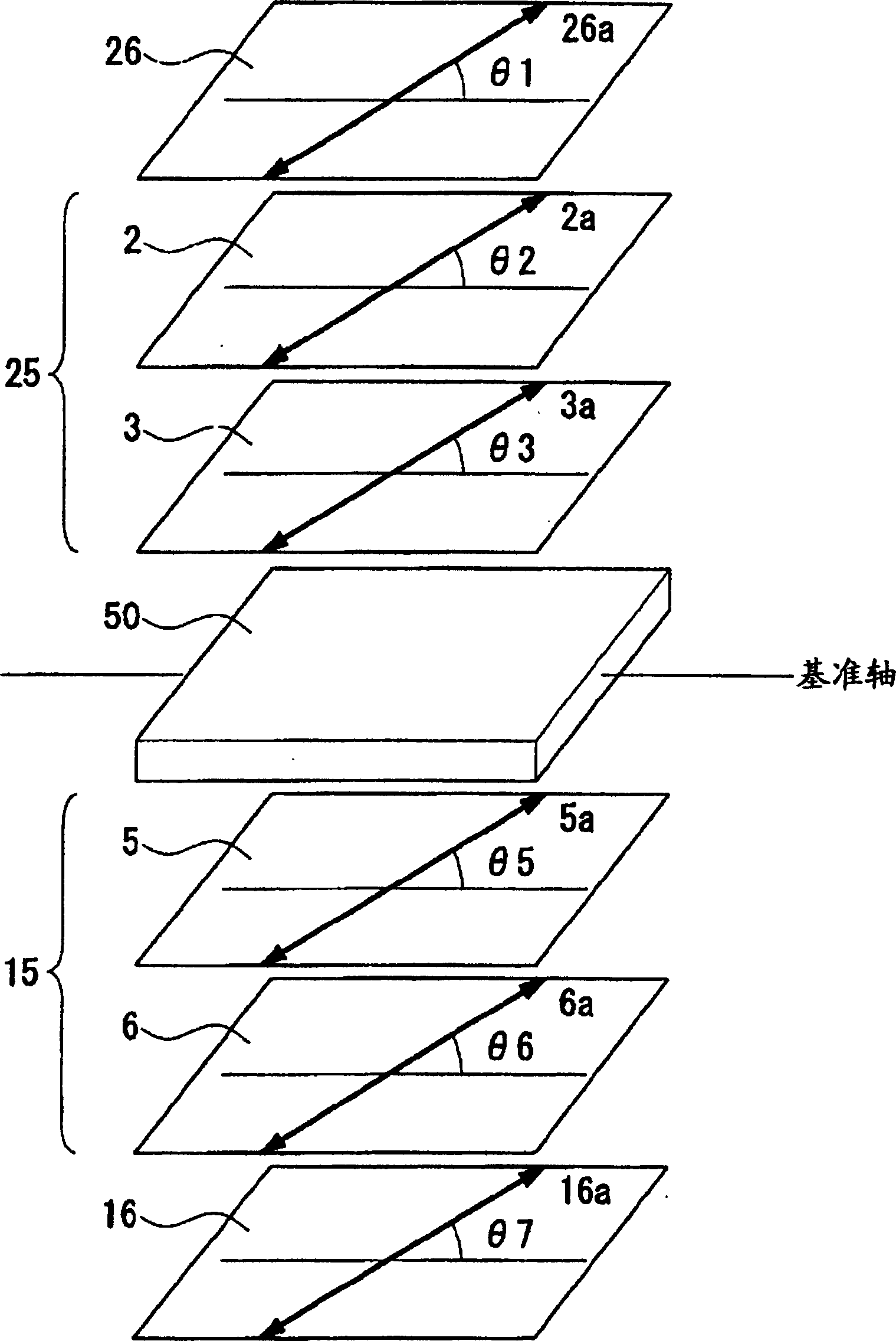
[0059] Below, refer to Figure 10 The liquid crystal display device of the second embodiment will be described. in addition, Figure 10 is equivalent to the first embodiment image 3 diagram.
[0060] The liquid crystal display device of the second embodiment is the same as the first embodiment, and it is an active matrix type transflective liquid crystal display device, such as Figure 10 As shown, the structures of the retardation plate and the polarizing plate provided on the respective substrates arranged at intervals of the liquid crystal layer 50 are different from those of the first embodiment. Therefore, configurations other than the configurations of the retardation plate and the polarizing plate are the same as those of the first embodiment, and thus description thereof will be omitted.
[0061] In this embodiment, the retardation plate 115 and the linear polarizing plate 116 as an elliptically polarizing plate are disposed on the backlight side (the outer surfac...
PUM
| Property | Measurement | Unit |
|---|---|---|
| angle | aaaaa | aaaaa |
Abstract
Description
Claims
Application Information


