

Layout method of semiconductor integrated circuit, layout structure thereof, and photomask for forming the layout structure
一种集成电路、布局结构的技术,应用在半导体集成电路的光掩模领域,能够解决抗蚀构图维度偏移、焦点偏移、暴光光强度偏移等问题
- Summary
- Abstract
- Description
- Claims
- Application Information
AI Technical Summary
Problems solved by technology
Method used
Image

Examples
Embodiment Construction
[0167] Exemplary embodiments according to the present invention will now be described with reference to the accompanying drawings.
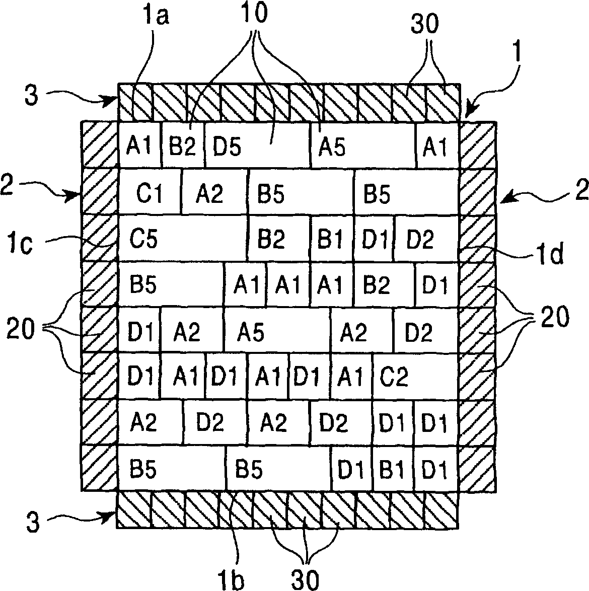
[0168] figure 1 An example of the layout structure of the semiconductor integrated circuit according to the present invention is shown.
[0169] figure 1 The illustrated layout structure includes a standard cell array 1 , a first adjacent dummy strip 2 along the vertical side of the standard cell array, and a second adjacent dummy strip 3 along the horizontal side of the standard cell array. A plurality of standard cells 10 distributed in the form of rows and columns forms a standard cell array 1 . The distributed multiple first adjacent dummy cells 20 form a first adjacent dummy strip 2 , and the distributed multiple second adjacent dummy cells 30 form a second adjacent dummy stripe 3 .
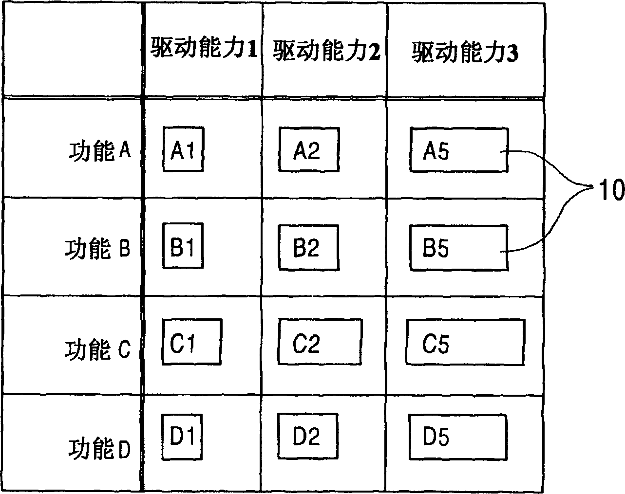
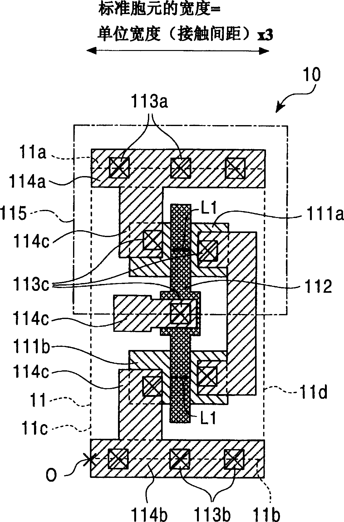
[0170] Each standard cell 10 has a circuit pattern (standard cell pattern), and has basic logic functions such as gates and flip-flops. The standard cell 1...
PUM
| Property | Measurement | Unit |
|---|---|---|
| wavelength | aaaaa | aaaaa |
Abstract
Description
Claims
Application Information