Method of forming junction isolation active assembly

A technology of active components and junction insulation, which is applied in the direction of electrical components, semiconductor/solid-state device manufacturing, circuits, etc., and can solve the problems of complex trench process, high cost, and affecting the reliability and quality of components

Inactive Publication Date: 2005-03-23
MACRONIX INT CO LTD
View PDF0 Cites 7 Cited by
  • Summary
  • Abstract
  • Description
  • Claims
  • Application Information

AI Technical Summary

Problems solved by technology

[0004] Since the trench process described above requires an etch process, a deposition-fill process, and a planarization process, there are many disadvantages
For example, the trench process is quite complex and costly, voids are ea...

Method used


Image

  • Method of forming junction isolation active assembly
  • Method of forming junction isolation active assembly
  • Method of forming junction isolation active assembly

Examples


Embodiment Construction

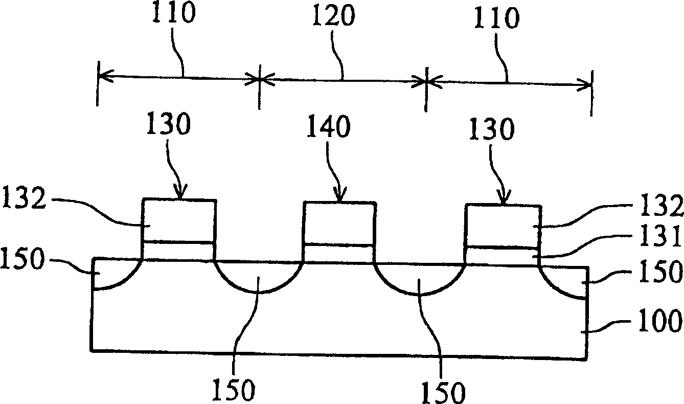
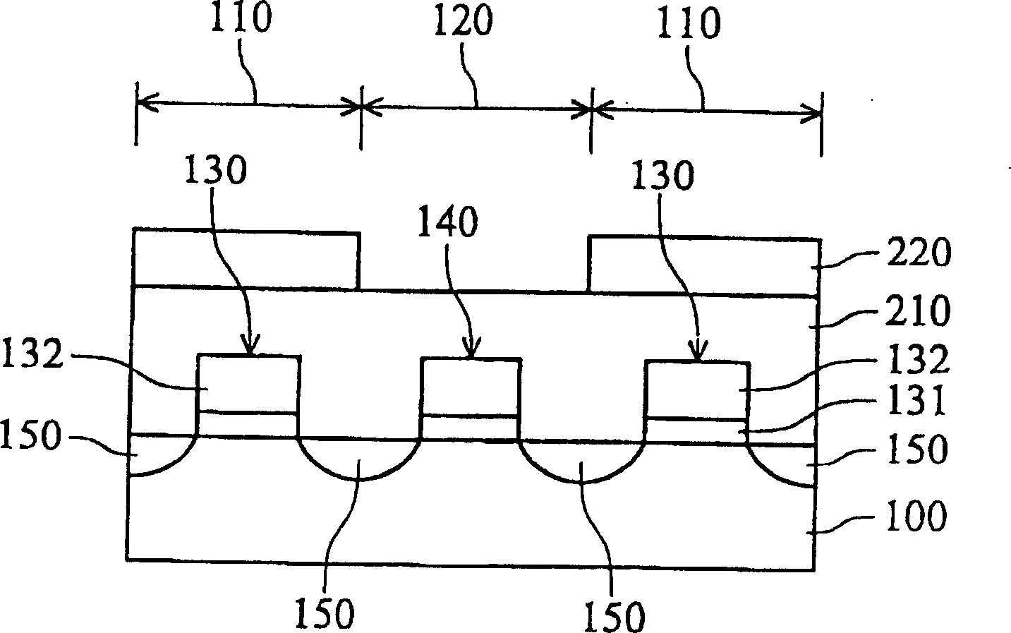
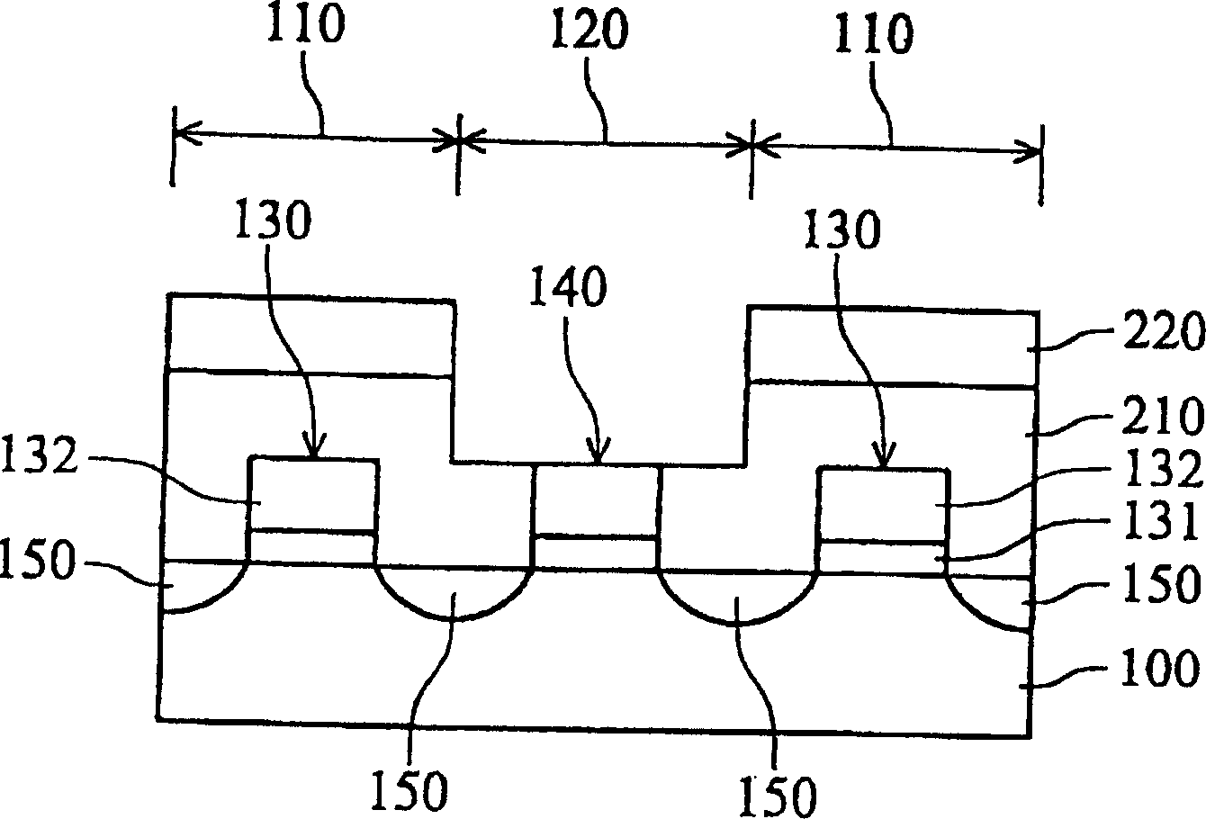
[0010] Use the following Figure 1~6 The process cross-sectional view is shown to illustrate an embodiment of the present invention.

[0011] First, if figure 1 As shown, it provides a semiconductor substrate 100, such as silicon, with a plurality of predetermined active regions (active areas) 110 on the substrate 100, and at least one predetermined isolation region (an isolation area) 120.

[0012] exist figure 1 In this method, a first gate structure 130 is formed on a part of the substrate 100 in the active region 110 , and a second gate structure 140 is formed on the substrate 100 in the isolation region 120 . An example is given here to illustrate the process of forming the first and second gate structures 130, 140. First, thermal oxidation or deposition is used to form, for example, SiO 2 An insulating layer (not shown) is on the substrate 100, and then a conductive layer (not shown) such as a polysilicon layer is formed on the insulating layer by deposition. Then...


PUM


Abstract

The invention provides a shaping method of the junction insulation active blocks. The fundus of the semiconductor has several preconcerted active regions and there is at least one preconcerted isolation region between the two active regions. It forms the first grid structure on part of the fundus of the active regions as well as the second grid structure on the fundus of the isolation regions, engenders the first ion adulterating region in the funduses of the two sides of the first and second grid structures, forms the antireflection coatings on the fundus and the first and second grid structures, gets rid of part of the antireflection coating to reveal the second grid structure, then get rid of the second grid structure to reveal the fundus, forms the second ion adulterating region in the fundus of the isolation area and gets rid of the antireflection coatings.

Description

technical field [0001] The invention relates to semiconductor integrated circuit technology, in particular to a method for forming a junction-insulated active component. Background technique [0002] In an integrated circuit device, active components that are isolated from each other are included. Therefore, the component isolation process has become an important part of the semiconductor process. [0003] Shallow trench isolation (shallow trench isolation, STI) or deep trench isolation has been often used in device isolation processes. The manufacturing method first uses dry etching to remove part of the silicon substrate to form a trench, then uses a deposition method to fill the trench with dielectric materials, and then uses, for example, chemical mechanical polishing to planarize the contour of the trench surface. [0004] Since the trench process described above requires an etching process, a deposition-filling process, and a planarization process, there are many dis...

Claims


Application Information

Patent Timeline
IPC IPC(8): H01L21/76H01L21/822H01L21/8234
Inventor 王俊淇苏俊联吕文彬
Owner MACRONIX INT CO LTD
Why Eureka
Try Eureka