GaN based LED upside down welding combination, and lamp and chip horizontally upside down welding technique

An inverted chip technology, applied to electrical components, electrical solid devices, circuits, etc., can solve the problems of low light extraction efficiency, lattice mismatch, expensive equipment, etc., and achieve simple production process, high current density, and current distribution. uniform effect

Inactive Publication Date: 2005-05-25
金芃
View PDF5 Cites 15 Cited by
  • Summary
  • Abstract
  • Description
  • Claims
  • Application Information

AI Technical Summary

Problems solved by technology

[0002] Chip-level upside-down welding process, especially for high-power GaN-based light-emitting diodes (LEDs), has the following disadvantages: (1) The process is complicated, the equipment is expensive, and the production efficiency is low. This is a low-cost mass production The bottleneck of high-power GaN-based light-emitting diodes; (2) due to the use of organic filling materials, the heat dissipation efficiency is not as expected; (3) the lattice mismatch between the substrate wafer and the epitaxial layer still exists; (4) the lining Inefficient light extraction due to total internal reflection between the bottom wafer and the epitaxial layer
GaN-based semiconductor light-emitting diodes can be epitaxially grown on GaN substrate wafers to avoid lattice mismatch, but GaN substrate wafers are very expensive
[0006] Total internal reflection greatly reduces light extraction efficiency

Method used


Image

  • GaN based LED upside down welding combination, and lamp and chip horizontally upside down welding technique
  • GaN based LED upside down welding combination, and lamp and chip horizontally upside down welding technique
  • GaN based LED upside down welding combination, and lamp and chip horizontally upside down welding technique

Examples


Embodiment Construction

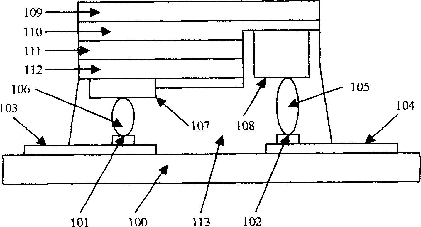
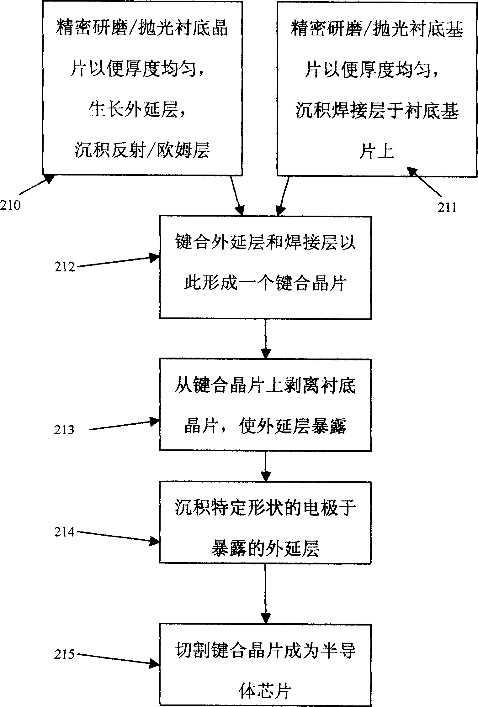
[0073] Figure 2a 2e to 2e show an implementation example of a wafer-level flip-bonding process method for producing a semiconductor chip or device flip-bonding assembly.

[0074] Figure 2a It is a process flow chart of wafer level upside-down welding in the present invention. Process steps 210 / 211, 212, 213, and 214 correspond to Figures 2b, 2c, 2d, and 2e, respectively. Process step 215 is dicing.

[0075] FIG. 2 b shows the preparation of the substrate wafer and substrate wafer 204 . The epitaxial layer 201 is grown on the sapphire substrate wafer 200 . Reflective and ohmic layer 202 is deposited on epitaxial layer 201 . First and second solder layers 203 and 205 are deposited on both sides of the substrate substrate 204, respectively.

[0076] The substrate wafer 200 may also be a GaN wafer, Si wafer or others. The material of the reflection layer is selected from the following materials: Al, Au, Ag and others. The reflective layer may also be a Bragg mirror. Subst...


PUM


Abstract

The invention discloses a novel high-power semiconductor chip or device (including a GaN-based light-emitting diode) upside-down welding assembly and a lamp, as well as a low-cost wafer-level upside down welding manufacturing process. It belongs to the technical field of semiconductor optoelectronics. The invention includes: the epitaxial layer of the semiconductor chip or device is welded upside down to the substrate, the substrate wafer is peeled off, electrodes of a specific shape are deposited on the epitaxial layer, the semiconductor chip or device is cut into a combination of upside down welding, and a new type of lamp is designed so that Reduce total internal reflection. The advantages of the present invention are: (1) The manufacturing process is simple; (2) No need for expensive chip-level flip welding equipment; (3) High production efficiency; (4) Good heat dissipation efficiency; (5) Current distribution Uniform, the current density is increased; (6) the light extraction efficiency is improved; (7) the total internal reflection is removed.

Description

technical field [0001] The invention discloses a new type of high-power semiconductor chip or device (including GaN-based light-emitting diode (LED)) upside-down welding combination and a lamp, and a wafer-level upside-down welding process method for producing a new type of high-power semiconductor chip or device upside down welding combination. Background technique [0002] The chip-level flip welding process method, especially for high-power GaN-based light-emitting diodes (LEDs), has the following disadvantages: (1) the process method is complicated, the equipment is expensive, and the production efficiency is low. This is a low-cost mass production method. The bottleneck of high-power GaN-based light-emitting diodes; (2) due to the use of organic filling materials, the heat dissipation efficiency is not as expected; (3) the lattice mismatch between the substrate wafer and the epitaxial layer still exists; (4) the lining Total internal reflection between the base wafer an...

Claims


Application Information

Patent Timeline
Patent Type & Authority Applications(China)
IPC IPC(8): H01L21/00H01L21/44H01L23/02H01L29/40H01L33/00H01L33/38H01L33/62
CPCH01L33/38H01L33/62H01L2924/01004H01L2924/01079H01L2224/48091H01L2924/12041H01L2924/10253H01L2224/05573H01L2224/05568H01L2924/00014H01L2224/16238H01L24/05H01L2224/0603H01L2224/06102H01L2224/1703H01L33/0093H01L2924/00H01L2224/05599H01L2224/16
Inventor 彭晖彭刚
Owner 金芃
Why Eureka
Try Eureka