Chip ball grid array packaging structure

A technology of ball grid array and packaging structure, which is applied in the direction of electrical components, electric solid devices, circuits, etc., and can solve the problems affecting the heat dissipation effect

Inactive Publication Date: 2005-06-22
ASE ASSEMBLY & TEST SHANGHAI
View PDF0 Cites 34 Cited by
  • Summary
  • Abstract
  • Description
  • Claims
  • Application Information

AI Technical Summary

Problems solved by technology

Therefore, the heat generated by the chip cannot be directly transferred to the heat sink, which greatly affects the heat dissipation effect.

Method used


Image

  • Chip ball grid array packaging structure
  • Chip ball grid array packaging structure
  • Chip ball grid array packaging structure

Examples


Embodiment Construction

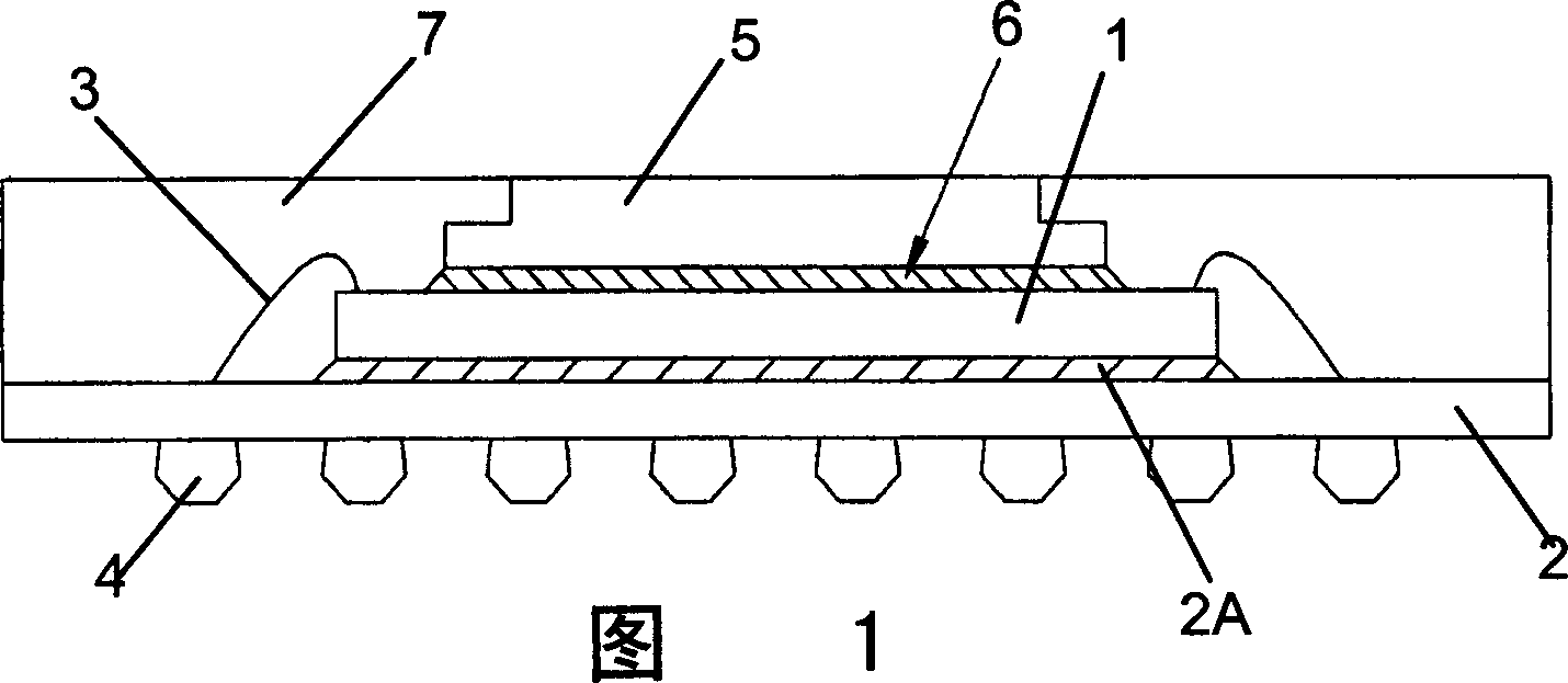
[0013] As shown in FIG. 1 , FIG. 1 shows a schematic diagram of a ball grid array package structure of the present invention. In FIG. 1, a chip 1 is bonded to a substrate 2 by an adhesive 2A or the like in a conventional method. Gold wires 3 electrically connect the circuitry on chip 1 to solder balls 4 under substrate 2 . The improvement of the present invention is that one side of the heat sink 5 is directly bonded to the surface of the chip 1 through the adhesive 6 . Then use the plastic package 7 to package the above-mentioned parts together.

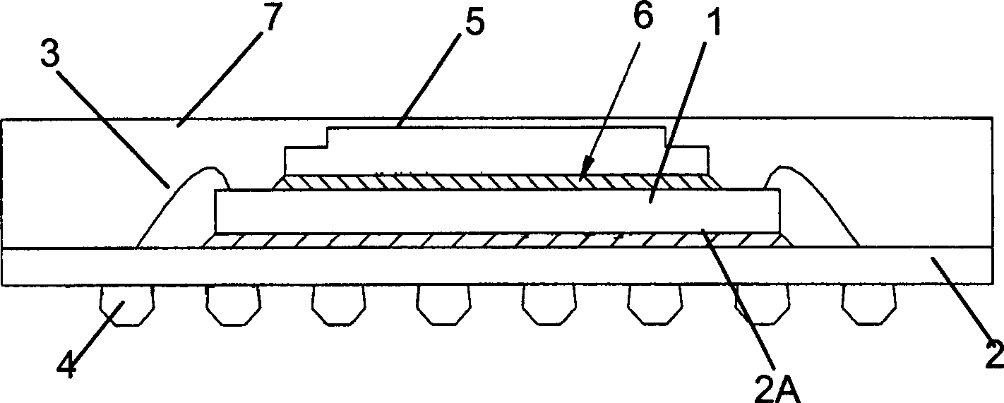
[0014] In the embodiment shown in FIG. 1 , the other surface of the heat sink 5 is exposed outside the plastic package 7 . Of course, you can also figure 2 In the illustrated embodiment, the heat sink 5 is not exposed outside the plastic package 7 .

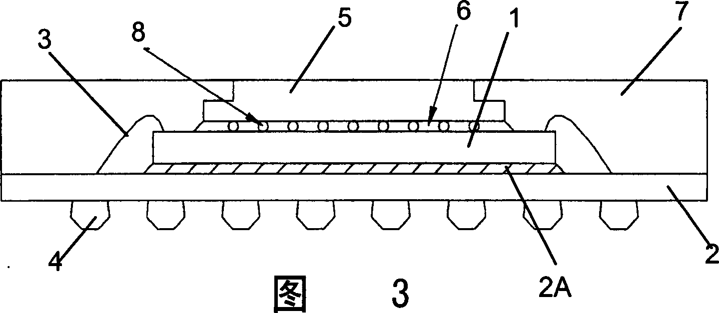
[0015] In Figure 1 and figure 2 In the shown embodiment, the adhesive 6 between the heat sink 5 and the chip 1 is an adhesive, however, as shown in FIG. 3 , some solid particles...


PUM


Abstract

This invention provides a package structure for chip ball grid array, which contains substrate, chip on substrate, radiation fin and plastic package body for packaging said substrate, chip and radiation fin wherein the radiation fin is adhered on chip by adherent to greatly improve the radiation property than current package.

Description

technical field [0001] The invention relates to a package structure of a chip, in particular to a ball grid array package structure of a chip, and mainly improves the package structure to improve the heat dissipation effect of the package structure. Background technique [0002] Chip ball grid array packaging structure (BGA) has been widely used in the current chip packaging field. However, the problem of heat dissipation hinders the further application of this package structure. The current packaging structure generally achieves heat dissipation by adding a heat sink, and the heat sink is in contact with the substrate and not in contact with the chip that generates heat. Therefore, the heat generated by the chip cannot be directly transmitted to the heat sink, which greatly affects the heat dissipation effect. Contents of the invention [0003] Therefore, the object of the present invention is to improve the BGA packaging structure to provide a chip BGA packaging struct...

Claims


Application Information

Patent Timeline
Patent Type & Authority Applications(China)
IPC IPC(8): H01L23/34
CPCH01L2224/32225H01L2224/48091H01L2224/48227H01L2224/73265H01L2924/15311H01L2924/181
Inventor 王涛
Owner ASE ASSEMBLY & TEST SHANGHAI
Why Eureka
Try Eureka