
Substrate processing apparatus and cleaning method therefor

一种处理器件、衬底的技术,应用在清洁方法和用具、化学仪器和方法、半导体/固态器件制造等方向,能够解决流动变乱、均匀性变差、难清洗等问题

Inactive Publication Date: 2005-07-13
PANASONIC CORP
View PDF1 Cites 26 Cited by
  • Summary
  • Abstract
  • Description
  • Claims
  • Application Information

AI Technical Summary

Problems solved by technology

[0010] In the above-mentioned conventional chemical vapor growth device, there is such a problem that as the number of times of film formation on the substrate 10 to be processed increases, the reaction product adheres to the gas holes on the baffle plate 14 and the plate 15, so by The flow of the reaction gas 21 in the gas hole is gradually disturbed, and as a result, the uniformity of the deposited film is deteriorated.
However, since the plasma 24 composed of the cleaning gas 23 is generated on the underside of the planar plate 15 (between the planar plate 15 and the substrate 10 to be processed), the surface of the baffle plate 14 (direction toward the substrate 10 to be processed) surface) and the backside of the planar plate 15 opposite to this surface (the surface opposite to the surface facing the direction of the substrate 10 to be processed) is difficult to be cleaned
Therefore, it is difficult to completely remove the reaction products attached to the gas holes of the baffle 14 and the panel 15 by plasma cleaning shown in FIG. 11( b ).

Method used


Image

  • Substrate processing apparatus and cleaning method therefor
  • Substrate processing apparatus and cleaning method therefor
  • Substrate processing apparatus and cleaning method therefor

Examples


no. 1 Embodiment

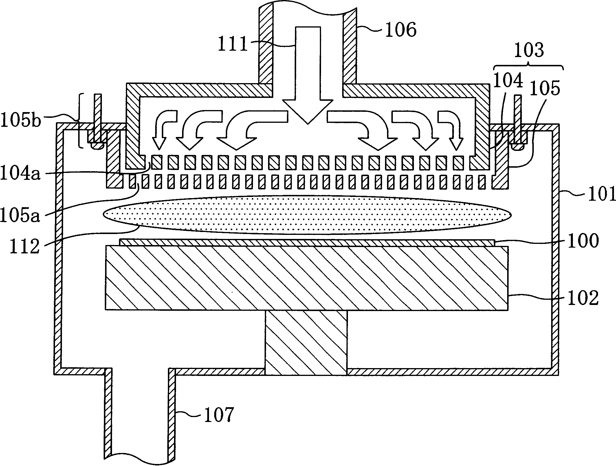
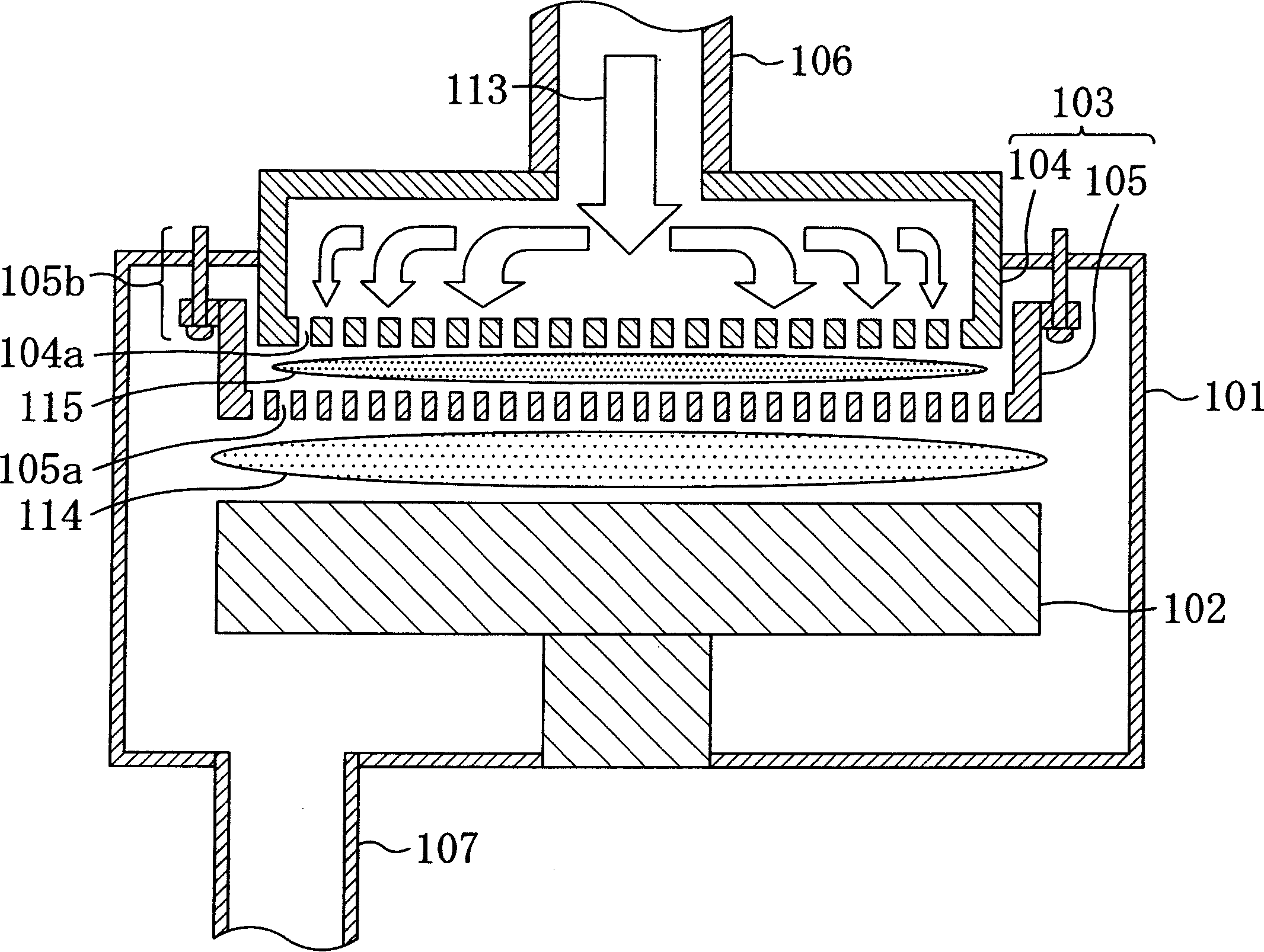
[0048] Hereinafter, the substrate processing device and its cleaning method according to the first embodiment of the present invention will be described with reference to the drawings.

[0049] figure 1 and figure 2 A schematic cross-sectional structure of a substrate processing device (specifically, a chemical vapor growth device) according to the first embodiment is shown; figure 1 Indicates the internal state of the device during film formation, figure 2 Indicates the internal state of the device at the time of cleaning.

[0050] Such as figure 1 and figure 2 As shown, a lower electrode 102 serving also as a substrate support is provided at the bottom of the reaction chamber 101 . That is, the processed substrate (wafer) 100 is mounted on the lower electrode 102 . In addition, the reaction chamber 101 is a reaction chamber capable of decompression (a pressure state lower than normal pressure (atmospheric pressure) can be realized), and the lower electrode 102 in...

no. 2 Embodiment

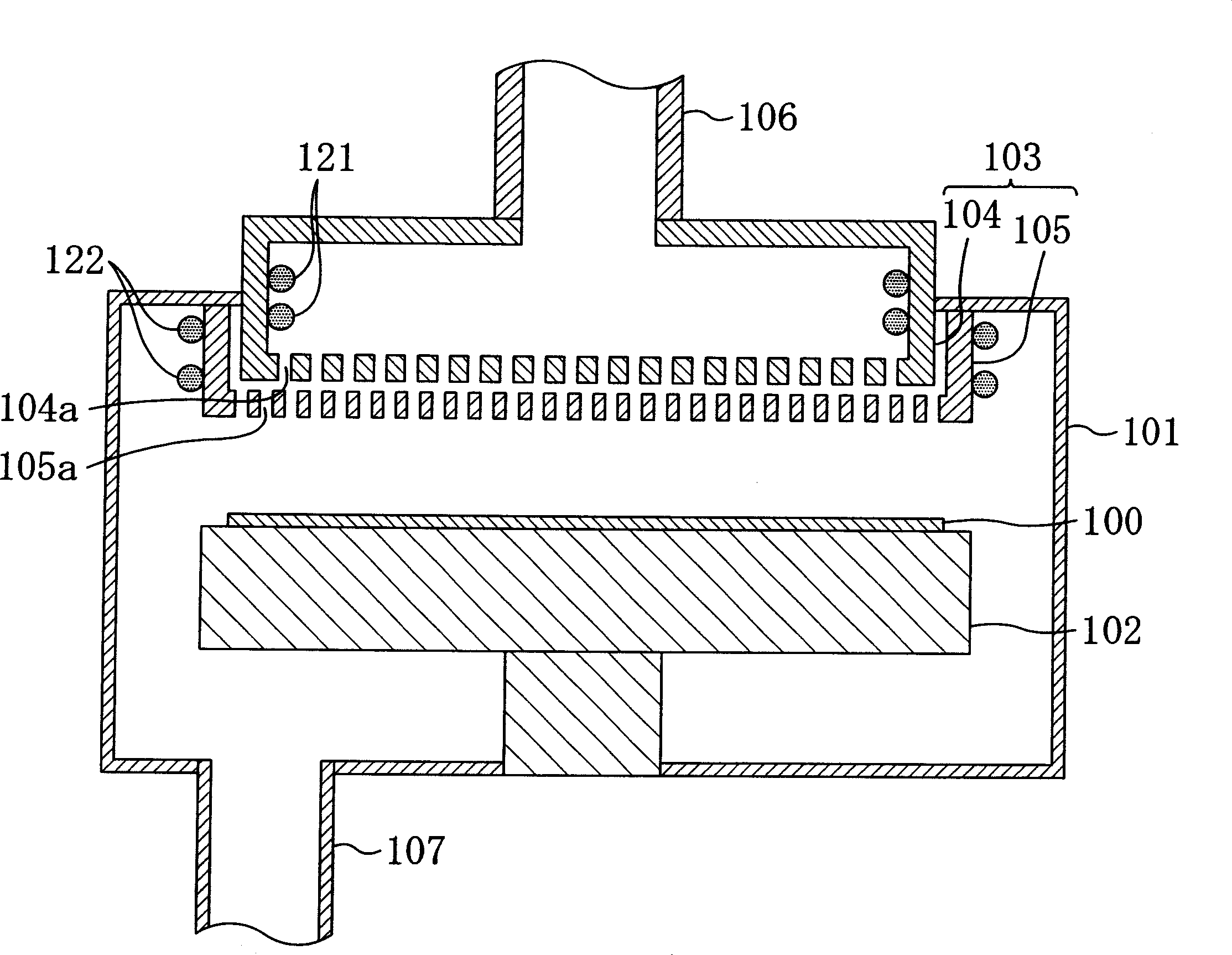
[0068] Hereinafter, a substrate processing device and a cleaning method thereof according to a second embodiment of the present invention will be described with reference to the drawings.

[0069] image 3 A schematic cross-sectional structure of a substrate processing device (specifically, a chemical vapor growth device) according to the second embodiment is shown. In addition, in image 3 in, for with figure 1 and figure 2 Components that are the same as in the first embodiment shown are denoted by the same symbols, and explanations thereof are omitted.

[0070] Such as image 3 As shown, in the substrate processing device of this embodiment, as in the first embodiment, the upper electrode 103 for generating plasma is composed of a baffle 104 and a flat plate 105. As a feature of this embodiment, the baffle The first heater 121 is attached to the inner wall surface of the side part of 104 , and the second heater 122 is attached to the outer wall surface of the side pa...

no. 3 Embodiment

[0077] Hereinafter, a substrate processing device and a cleaning method thereof according to a third embodiment of the present invention will be described with reference to the drawings.

[0078] Figure 4 A schematic cross-sectional structure of a substrate processing device (specifically, a chemical vapor growth device) according to the third embodiment is shown. In addition, in Figure 4 in, right with figure 1 and figure 2 Components that are the same as in the first embodiment shown are denoted by the same symbols, and explanations thereof are omitted.

[0079] Such as Figure 4 As shown, in the substrate processing device of this embodiment, as in the first embodiment, the upper electrode 103 for generating plasma is composed of a baffle plate 104 and a flat plate 105, but as a feature of this embodiment, it can The ultrasonic vibration source 131 that transmits ultrasonic vibrations to the baffle 104 , that is, the upper electrode 103 is fixedly installed on the ...


PUM


Abstract

The invention discloses a substrate processing device and a cleaning method thereof. The object of the present invention is to prevent the diameter of the gas hole from becoming narrower every time the film-forming process is repeated due to the adhesion of the reaction product to the inner wall of the gas hole of the gas shower for film formation in the chemical vapor growth device or the like. Phenomenon, preventing the film thickness uniformity of the formed film from deteriorating. Inside the reaction chamber 101, an upper electrode 103 serving also as a gas shower for film formation is provided. The upper electrode 103 is composed of a baffle 104 and a flat plate 105 . Among them, the baffle plate 104 has holes 104 a for dispersing the gas introduced into the reaction chamber 101 , and the flat plate 105 has holes 105 a for further dispersing the gas dispersed by the baffle plate 104 . When cleaning the reaction product, the gap between the two plates is increased using the mechanism 105b and a high-frequency voltage is applied between the two plates to generate plasma 114 composed of cleaning gas 113 .

Description

technical field [0001] The present invention relates to a substrate processing device, in particular to an internal structure related to cleaning in a chemical vapor growth device for forming thin films for semiconductor devices, and a cleaning method for the chemical vapor growth device having the structure. Background technique [0002] In recent years, higher integration, lower power consumption, and lower cost of semiconductor devices have been progressing. In order to achieve high integration, low power consumption, and low cost, thinner and more uniform films are urgently required as insulating films constituting semiconductor devices. [0003] Figure 11(a) and (b) show the schematic cross-sectional structure of a conventional monolithic chemical vapor growth device, Figure 11(a) shows the state inside the device during film formation, and Figure 11(b) shows the state inside the device during cleaning (Refer to Japanese Patent Application Laid-Open No. 2000-273638). ...

Claims


Application Information

Patent Timeline
Patent Type & Authority Applications(China)
IPC IPC(8): C23C16/44C23C16/455H01L21/3065H01L21/31
CPCC23C16/4405C23C16/45565
Inventor 松原俊夫上田聪佐藤宏行内岛秀人
Owner PANASONIC CORP
Learn More