Board-level EMI shield with enhanced thermal dissipation

A board-level, substrate technology, applied in the field of board-level electromagnetic interference shielding, can solve problems such as increasing weight, not allowing mutual shielding, and consuming valuable PCB space

Inactive Publication Date: 2005-08-24
WL GORE & ASSOC INC
View PDF2 Cites 30 Cited by
  • Summary
  • Abstract
  • Description
  • Claims
  • Application Information

AI Technical Summary

Problems solved by technology

However, the shielding schemes in both of these references are not board-level because they do not allow areas of the same PCB to be shielded from each other (i.e., one chip to another)
Additionally, these solutions require attachment mechanisms involving screws or bolts and holes through the PCB
This consumes valuable PCB space and adds weight to the design

Method used


Image

  • Board-level EMI shield with enhanced thermal dissipation
  • Board-level EMI shield with enhanced thermal dissipation
  • Board-level EMI shield with enhanced thermal dissipation

Examples


Embodiment Construction

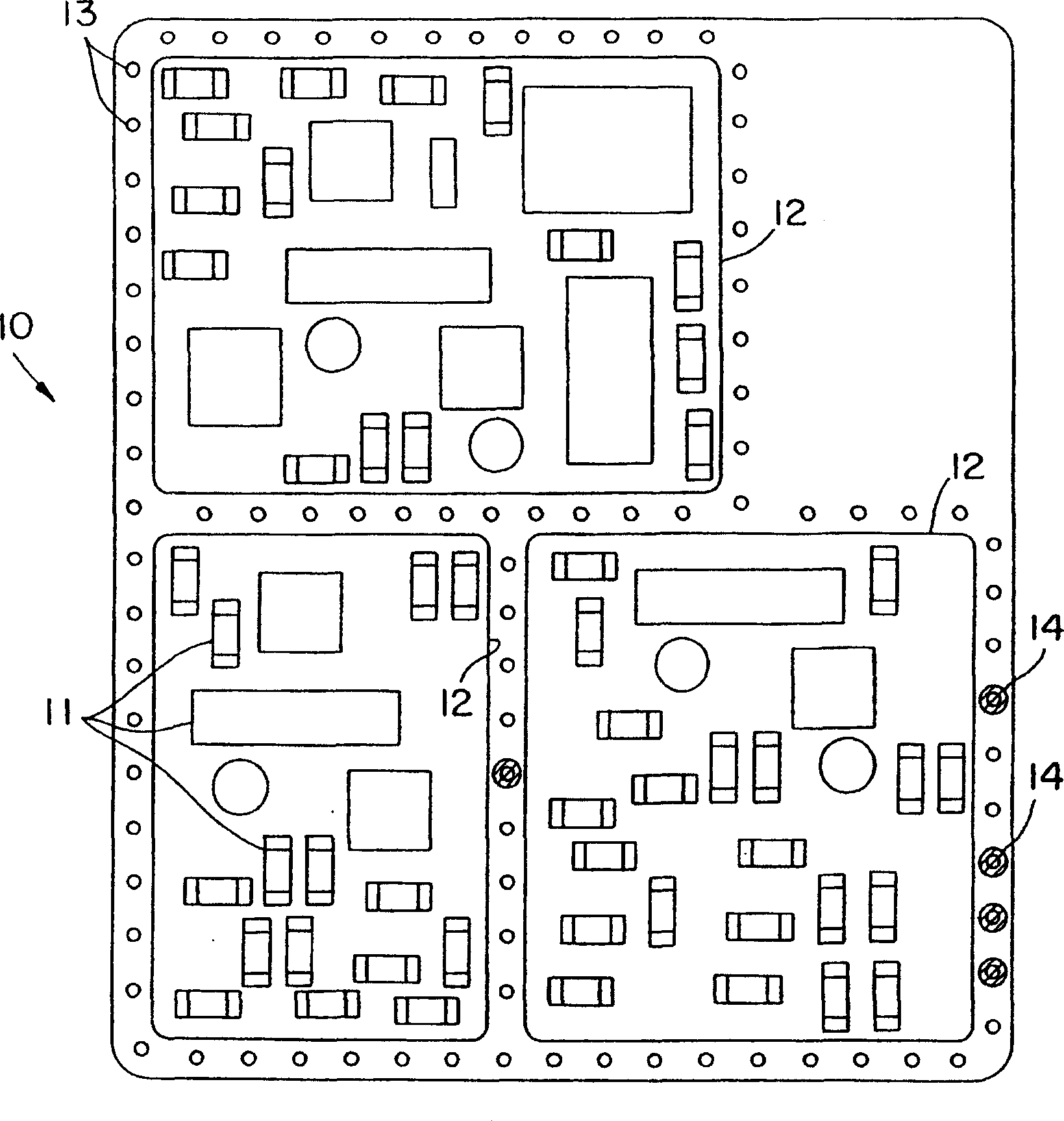
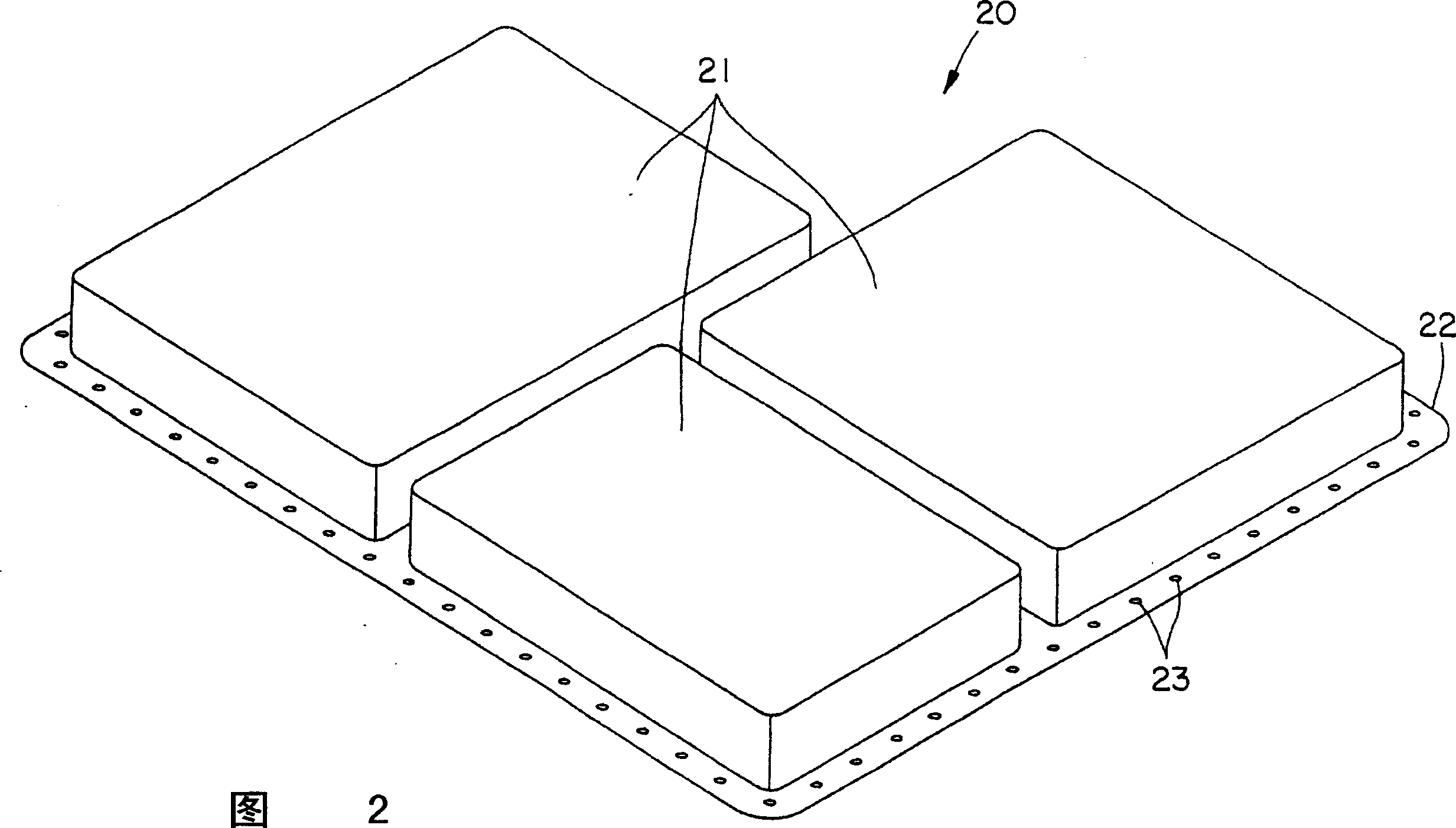
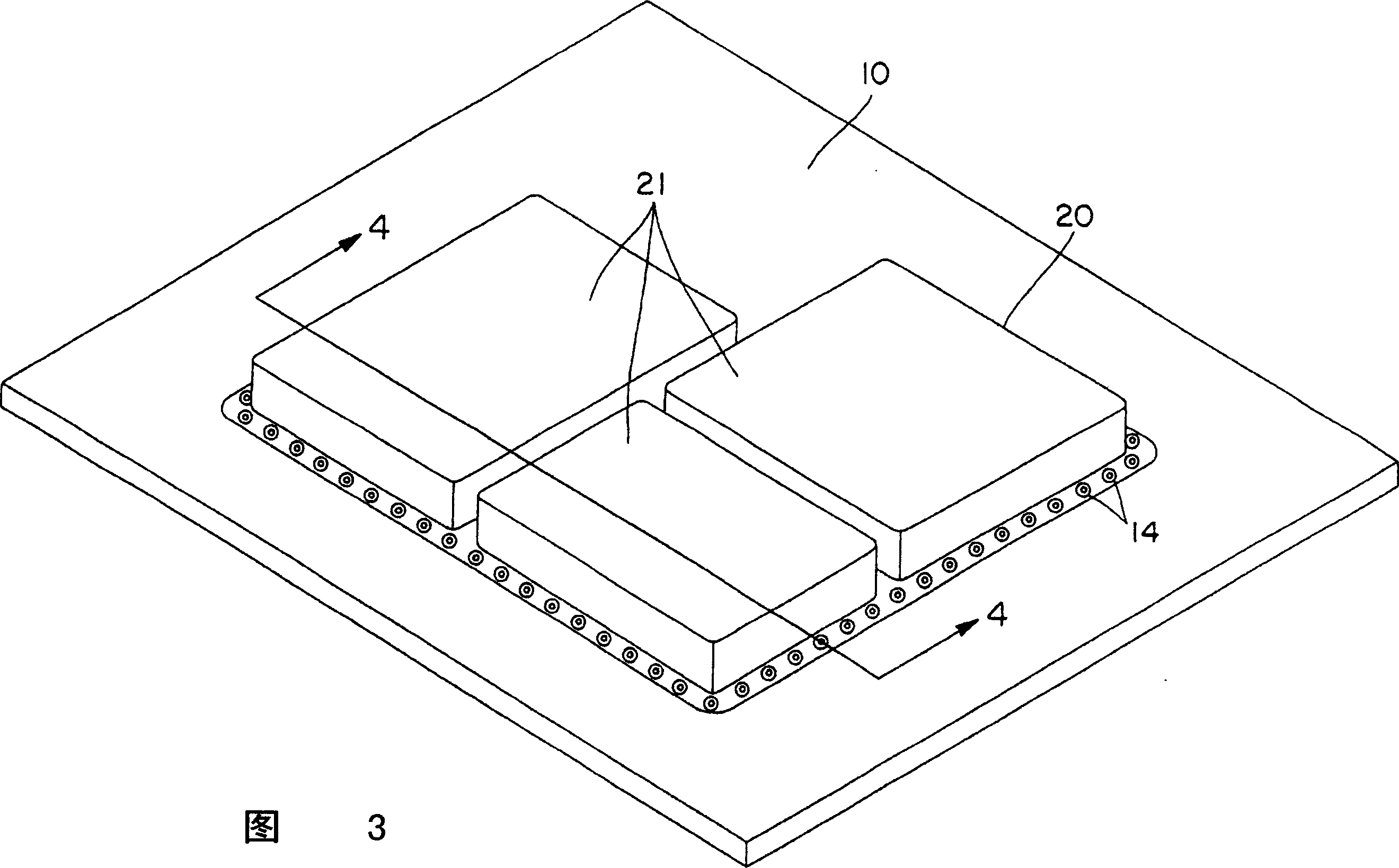
[0022] Referring now to the drawings, the present invention provides board level EMI shielding that enhances heat dissipation from shielded components. figure 1 is a plan view of a PCB (10) according to an embodiment of the present invention. A PCB (10) is a substrate having a plurality of electrical components (11) grouped together in an area (12). Surrounding the area (12) are a plurality of ground trace pads (13). Disposed on each ground track pad (13) is a conductive fastening unit (14). The conductive fastening unit (14) is mechanically and electrically coupled to the ground trace pad (13), for example by using solder. For ease of illustration, only some ground trace pads (13) are shown to have conductive fastening units (14) disposed thereon, but preferably, all ground trace pads (13) have conductive fastening units (14) disposed thereon. permanent fastening unit (14). A plurality of discrete conductive fastening units (14) are arranged on the PCB (10) in a pattern s...


PUM


Abstract

A substrate having at least one electrical component disposed thereon; a plurality of discrete electrically conductive fastening units disposed in a pattern on the substrate surrounding the at least one electrical component; a board-level electromagnetic interference (EMI) shield comprising an electrically conductive layer; a plurality of apertures formed in the board-level EMI shield such that the apertures correspond to the pattern of the electrically conductive fastening units; with at least one thermally conductive interface (TCI) material disposed over the at least one electrical component; and wherein the electrically conductive layer of the board-level EMI shield is in electrical contact with at least one electrically conductive fastening unit.

Description

field of invention [0001] The present invention generally relates to improved board-level electromagnetic interference (EMI) shielding for use in applications where heat dissipation is important. In particular, the present invention relates to a shield that is easy to disassemble, compatible with single or multi-compartment shield designs, has thinner sides, is lighter in weight and supports improved heat dissipation of the shield elements. This solution is particularly advantageous for use in smaller electronic devices, such as mobile phones, personal digital assistants, handheld and laptop computers, and the like. Background of the invention [0002] EMI shielding limits electromagnetic radiation from entering or leaving the area of ​​a printed circuit board (PCB) that contains electronic components. An EMI shield is further defined as "board level" if it is attached directly to the PCB surface with no external or free fixtures such as screws or bolts, thereby removing a ...

Claims


Application Information

Patent Timeline
Patent Type & Authority Applications(China)
IPC IPC(8): H01L23/552H05K7/20H05K9/00
CPCH01L2924/16152H01L2924/01079H01L23/552H01L2224/32245H01L2224/16H05K9/0026H05K9/003H01L2224/73253H01L2924/01078H01L2924/16153H05K7/20445H01L2924/01087H01L2224/16225H01L2924/3025H05K9/0035H05K9/0028H05K9/00H05K7/20
Inventor B·雷斯W·坎笛
Owner WL GORE & ASSOC INC
Why Eureka
Try Eureka