Method and apparatus for improving PCB design efficiency

A design efficiency and design tool technology, applied in the computer field, can solve the problems of increased PCB design error rate, large workload, long layout design time, etc., to reduce workload, improve efficiency, and reduce complexity.

Inactive Publication Date: 2005-09-14
广州博士科技交流中心有限公司
View PDF0 Cites 19 Cited by
  • Summary
  • Abstract
  • Description
  • Claims
  • Application Information

AI Technical Summary

Problems solved by technology

[0004] In short, the methods adopted in the above-mentioned prior art all fail to effectively utilize the location information of the devices in the schematic diagram, resulting in the fai

Method used


Image

  • Method and apparatus for improving PCB design efficiency
  • Method and apparatus for improving PCB design efficiency
  • Method and apparatus for improving PCB design efficiency

Examples


Embodiment Construction

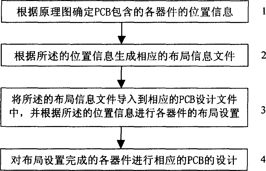
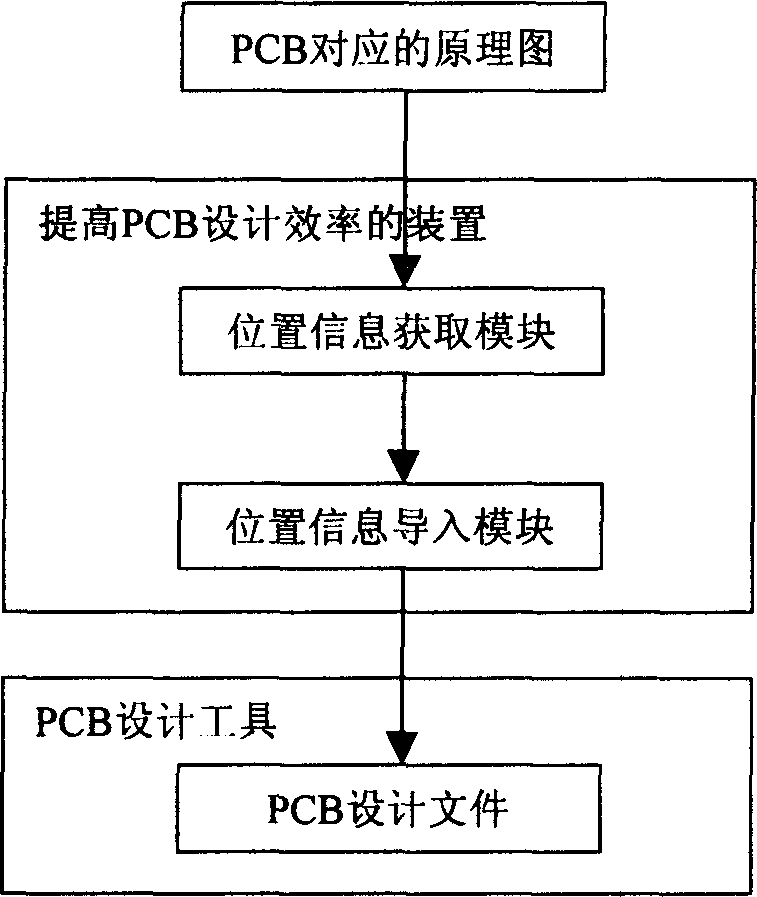
[0035] The invention mainly brings the position information of devices in the PCB schematic diagram into PCB design, so that the PCB design is realized based on the position information of each device in the PCB schematic diagram, thereby doubling the efficiency of PCB layout design.

[0036] In the PCB, if the relative position of each device is the same as that of the device in the schematic diagram. As an ordinary PCB design engineer, it is easy to understand the relationship between them and the required layout position only by looking at the relative positions of the devices in the PCB diagram. In this way, the layout of more than 95% of the devices can be completed almost without using the schematic diagram when the PCB is laid out, which greatly improves the design efficiency. Although the PCB package size of a device may be quite different from the size of the mark in the schematic diagram, the inconsistency of the device size will not affect the PCB design engineer's ...


PUM


Abstract

The invention relates to a method and its device that can enhance efficiency of PCB (printed circuit board) design. The invention introduces position information of various components in elementary diagram according to PCB to layout-planning process of PCB design files, so the arrangement of PCB design files is no longer the random arrangement of components that overlap in a large number. In this invention, position information of various components in PCB elementary diagram is led in design files by relative software, then designer can see the fairly clear relative position of various components in PCB from the corresponding PCB design files.

Description

technical field [0001] The invention relates to the technical field of computers, in particular to a method and a device for improving PCB (printed circuit board) design efficiency. Background technique [0002] The PCB design needs to be realized according to the corresponding circuit schematic diagram. Take an ordinary communication system user board as an example, the principle Figure 1 Usually 50 to 100 pages. There are 3,000 to 5,000 devices in one pack. At present, only the netlist is the only information transfer in the process from the schematic diagram to the PCB design, and the netlist only includes device packaging information and connection information, but does not include any device layout information, that is, does not include device location information. This makes the initial layout of thousands of devices in the PCB completely overlapped or randomly arranged in the process of PCB design according to the netlist. For this reason, PCB designers need to in...

Claims


Application Information

Patent Timeline
IPC IPC(8): G06F17/50
Inventor 李广生
Owner 广州博士科技交流中心有限公司
Why Eureka
Try Eureka