Semiconductor device and manufacturing method thereof, and liquid crystal module and semiconductor module having the same

A manufacturing method and semiconductor technology, which is applied in semiconductor/solid-state device manufacturing, semiconductor devices, semiconductor/solid-state device components, etc., can solve problems such as reduced reliability and poor device operation

Active Publication Date: 2005-09-28
SHENZHEN TOREY MICROELECTRONIC TECH CO LTD
View PDF3 Cites 20 Cited by
  • Summary
  • Abstract
  • Description
  • Claims
  • Application Information

AI Technical Summary

Problems solved by technology

[0019] When a voltage is applied, the semiconductor element 1 generates heat, and the smaller the heat capacity, the greater the temperature rise. In a high temperature state, the characteristics of the semiconductor element 1 change, which affects the operation of the device and may cause a decrease in reliability.

Method used


Image

  • Semiconductor device and manufacturing method thereof, and liquid crystal module and semiconductor module having the same
  • Semiconductor device and manufacturing method thereof, and liquid crystal module and semiconductor module having the same
  • Semiconductor device and manufacturing method thereof, and liquid crystal module and semiconductor module having the same

Examples


Embodiment 1

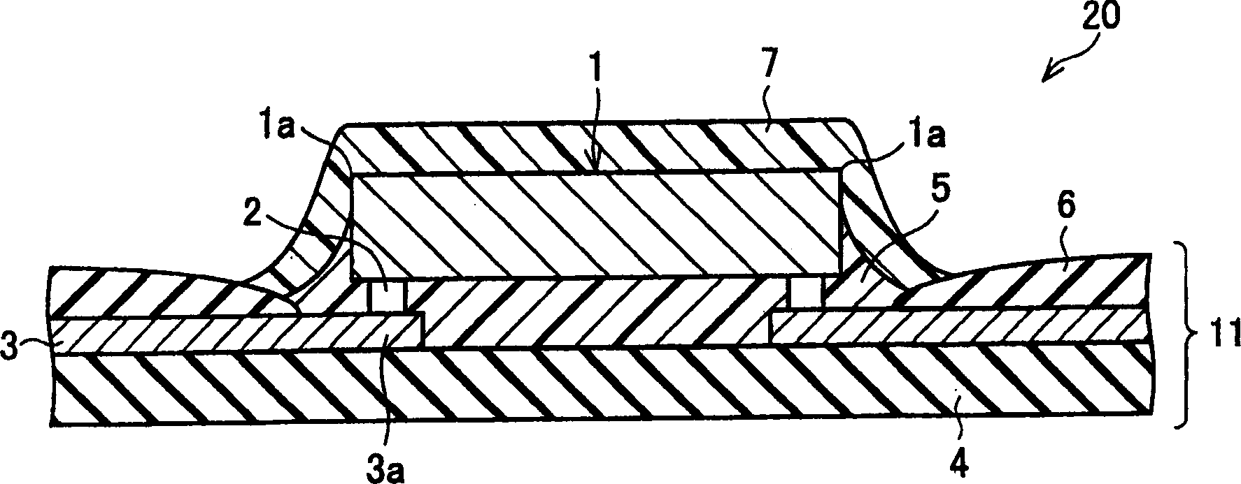
[0052] according to figure 1 And Fig. 7 (a), Fig. 7 (b), describe as follows with respect to an embodiment of the present invention.

[0053] figure 1 is a cross-sectional view showing a schematic structure of a semiconductor element mounting region in the semiconductor device of this embodiment.

[0054] like figure 1 As shown, the semiconductor device 20 of this embodiment is equipped with a wiring substrate 11 and a semiconductor element 1, and the semiconductor element 1 is mounted on the wiring substrate 11 using an underfill 5 as a first sealing resin layer, and at the same time, mounted on the wiring substrate 11. The back surface of the semiconductor element 1 on 11 has a structure completely covered with the top coat layer 7 as the second sealing resin layer.

[0055] The semiconductor element 1 described above is used for drive control of an electronic device in which the semiconductor device 20 is mounted. The above-mentioned semiconductor element 1 is formed...

Embodiment 2

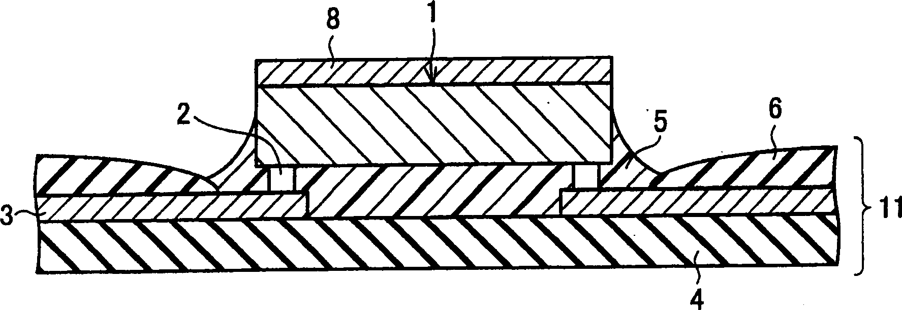
[0092] According to FIG. 2(a) and FIG. 2(b), an embodiment of the present invention is described as follows. In addition, for the convenience of description, the constituent elements having the same functions as those of the first embodiment are given the same reference numerals, and their descriptions are omitted. In this embodiment, differences from the first embodiment described above will be mainly described.

[0093] Fig. 2 (a) and Fig. 2 (b) are main part sectional views showing the manufacturing method of the semiconductor device of the present embodiment, and these Fig. 2 (a) and Fig. 2 (b) show the semiconductor device in the semiconductor device of the present embodiment Cross-section of the component packaging area.

[0094] As shown in Fig. 2 (a) and Fig. 2 (b), the semiconductor device 20 of the present embodiment has the upper surface (back side, i.e. with On the surface opposite to the active surface as the functional circuit surface, a metal plate 8 having hi...

Embodiment 3

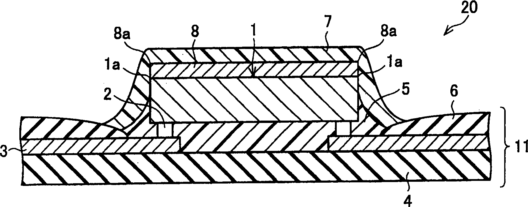
[0108] according to Figure 3(a) ~ Figure 3(c) and Figure 4 , an embodiment of the present invention is described as follows. In addition, for the convenience of description, the constituent elements having the same functions as those of Embodiments 1 and 2 are denoted by the same reference numerals, and their descriptions are omitted. In this embodiment, differences from the first embodiment described above will be mainly described.

[0109] Figure 3(a) ~ Figure 3(c) is a sectional view of main parts showing the method of manufacturing the semiconductor device of this embodiment, and these Figure 3(a) ~ Figure 3(c) A cross section of a semiconductor element mounting region in the semiconductor device of this embodiment is shown.

[0110] As shown in FIG. 3( c ), the semiconductor device 20 of this embodiment has the same structure as the semiconductor device 20 of the above-mentioned embodiment 2, but the manufacturing process is different.

[0111] Next, a method of ...


PUM

PropertyMeasurementUnit
thicknessaaaaaaaaaa

Abstract

Resin-sealing of a semiconductor element is carried out in two processes, by (I) forming a first sealing-resin layer by (i) sealing a connecting region of the semiconductor element and a wiring pattern with a first sealing resin, and (ii) curing the first sealing-resin, and then (II) forming a second sealing-resin layer by (i) providing the semiconductor element with a second sealing resin so that at least an edge portion of the semiconductor element is sealed, and (ii) curing the second sealing-resin. A semiconductor device thus obtained has a two-layer structure of the sealing-resin including (I) the first sealing-resin layer sealing the connecting region of the semiconductor element and the wiring pattern and (II) the second sealing-resin layer being so provided to the semiconductor element that at least an exposed edge portion of the semiconductor element is sealed.

Description

technical field [0001] The present invention relates to a film substrate provided with a wiring pattern and a semiconductor element mounted on the film substrate, the semiconductor element has a terminal for connection with the wiring pattern on an active surface, the connection terminal is opposite to the wiring pattern, A semiconductor device in which the above-mentioned semiconductor element is sealed with a sealing resin, a manufacturing method thereof, and a liquid crystal module and a semiconductor module equipped with the semiconductor device. Background technique [0002] In recent years, with the demand for miniaturization and thinning in semiconductor modules such as mobile phones and thin displays, semiconductor devices mounted in these semiconductor modules are also required to be miniaturized and thinned, and at the same time, further improvements in mounting density, mounting reliability. [0003] Therefore, in recent years, as a packaging technology for semic...

Claims


Application Information

Patent Timeline
Patent Type & Authority Applications(China)
IPC IPC(8): H01L23/29G02F1/13G02F1/136H01L21/56H01L23/12H01L23/28H01L23/31H01L23/48
CPCG02F1/13452H01L2224/16227H01L2924/07811H01L21/563H01L2224/16225H01L2224/73204H01L23/3135H01L2924/01078H01L2224/32225H01L2224/73203H01L2224/16H01L2924/01079H01L2924/00H01L21/56
Inventor 庄子裕史丰泽健司
Owner SHENZHEN TOREY MICROELECTRONIC TECH CO LTD
Why Eureka
Try Eureka