Semiconductor device and manufacturing method thereof

a semiconductor film and semiconductor technology, applied in the direction of semiconductor devices, electrical devices, transistors, etc., can solve the problems of the oxide semiconductor film's semiconductor characteristics, and achieve the reduction of hydrogen concentration and oxygen deficiency, excellent semiconductor characteristics, and reduced oxide semiconductor film oxygen deficiency

Active Publication Date: 2012-09-27
SEMICON ENERGY LAB CO LTD
View PDF4 Cites 30 Cited by
  • Summary
  • Abstract
  • Description
  • Claims
  • Application Information

AI Technical Summary

Benefits of technology

[0029]Further, it is preferable that the hydrogen permeable film be formed thin so that hydrogen released from the oxide semiconductor film by heat treatment efficiently diffuses (penetrates). Specifically, in the case where the hydrogen permeable film is a silicon oxide film or a silicon oxynitride film, the film thickness is greater than or equal to 0.5 nm and less than or equal to 15 nm, preferably greater than or equal to 2 nm and less than or equal to 5 nm.
[0030]In a semiconductor device which is one embodiment of the present invention and a method for manufacturing the semiconductor device, hydrogen exists in an oxide semiconductor film is released by heat treatment, and the hydrogen passes through a hydrogen permeable film and is captured by a hydrogen capture film. In other words, the heat treatment enables hydrogen contained in the oxide semiconductor film to transfer to the hydrogen capture film. Therefore, the oxide semiconductor film in the semiconductor device is an oxide semiconductor film whose hydrogen content is reduced. Further, with use of a film containing oxide (e.g., silicon oxide film or silicon oxynitride film) as the hydrogen permeable film, oxygen can be supplied to the oxide semiconductor film by the heat treatment, whereby oxygen deficiency in the oxide semiconductor film can be reduced.
[0031]According to one embodiment of the present invention, a semiconductor device including an oxide semiconductor film in which the hydrogen concentration and oxygen deficiency are reduced can be provided. The oxide semiconductor film has excellent semiconductor characteristics; therefore, according to one embodiment of the present invention, a semiconductor device having excellent electric characteristics can be provided.

Problems solved by technology

As described above, when hydrogen enter the oxide semiconductor film and conductivity is increased, a problem arises in semiconductor characteristics of the oxide semiconductor film.

Method used


Image

  • Semiconductor device and manufacturing method thereof
  • Semiconductor device and manufacturing method thereof
  • Semiconductor device and manufacturing method thereof

Examples


embodiment 1

[0051]In this embodiment, a semiconductor device which is one embodiment of the present invention will be described. Here, a transistor will be described as an example of the semiconductor device. The transistor may have a top-contact structure or a bottom-contact structure as long as it has a bottom-gate structure. A bottom-gate top-contact transistor will be described as an example in this embodiment.

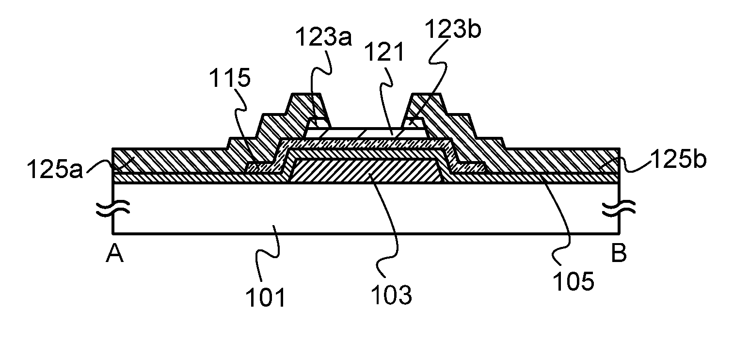
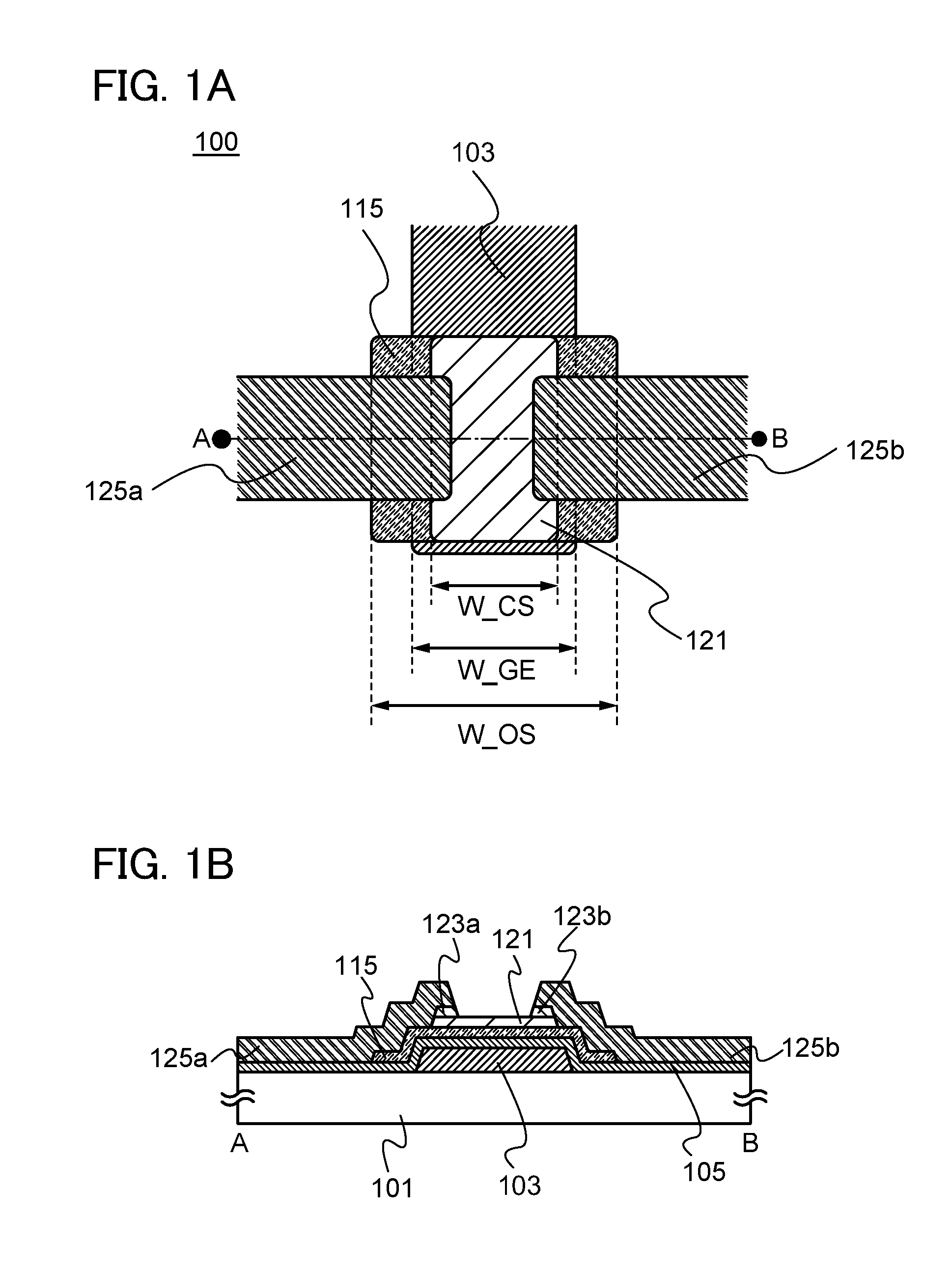
[0052]FIG. 1A is the top view of a transistor 100. FIG. 1B is the cross-sectional view taken along the alternate long and short dashed line A-B in FIG. 1A.

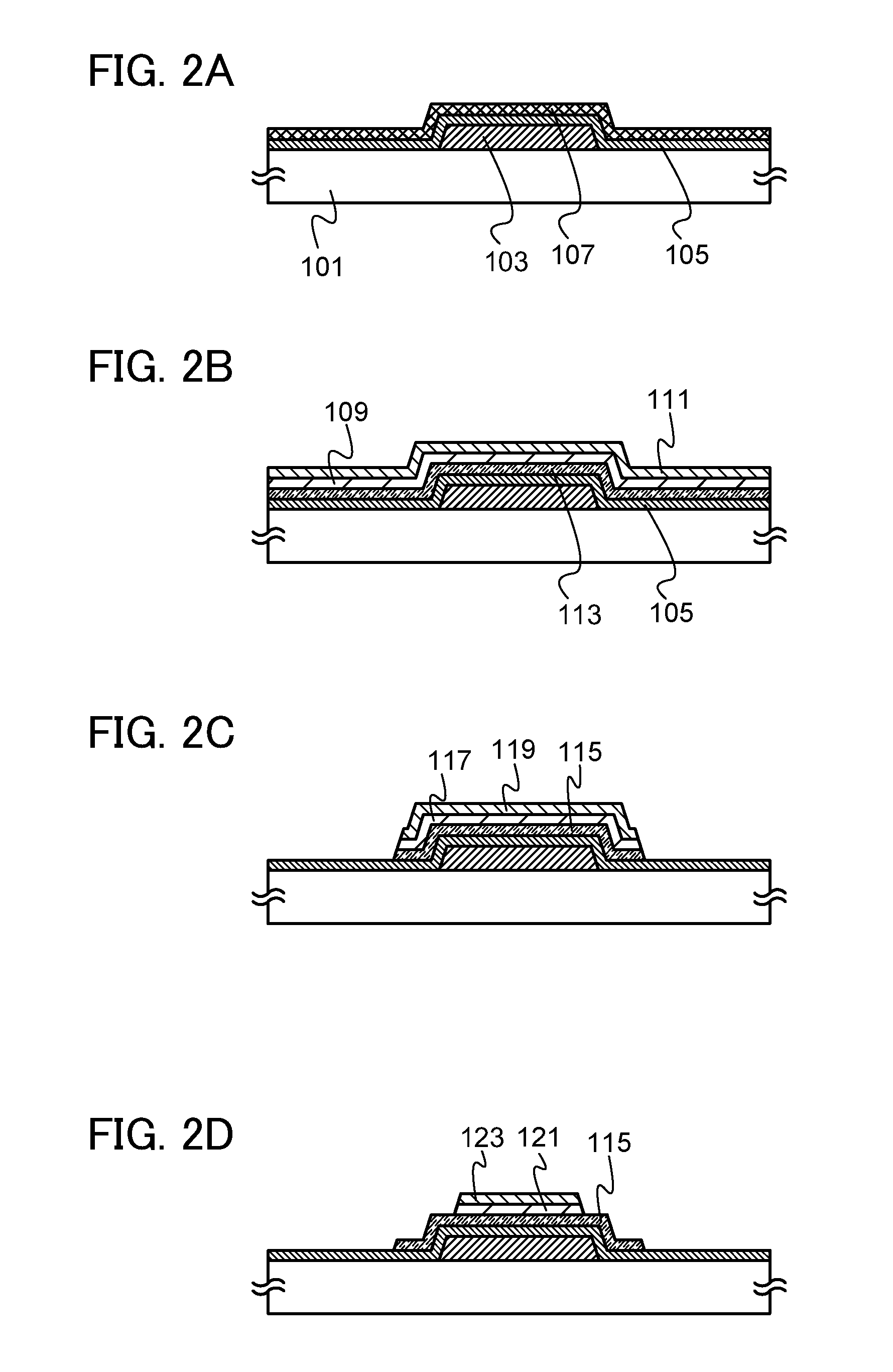
[0053]The transistor 100 includes a gate electrode 103 over a substrate 101, a gate insulating film 105 covering the gate electrode 103, an oxide semiconductor film 115 over the gate insulating film 105, a channel protective film 121 formed of a film having a hydrogen permeable property (a hydrogen permeable film) over the oxide semiconductor film 115, a source electrode 125a and a drain electrode 125b in contact with part of the ox...

embodiment 2

[0153]In this embodiment, a transistor 200 whose structure is partly different from the structure of the transistor 100 in Embodiment 1 will be described. Specifically, the transistor 200 differs from the transistor 100 only in the shape of the hydrogen capture film; therefore, reference numerals used for description of the transistor 200 are the same as those used for the description of the transistor 100 in some cases. In addition, the transistor 200 is one of modification examples of the transistor 100, so that the description in Embodiment 1 can be applied to this embodiment.

[0154]FIG. 4A is the top view of the transistor 200. FIG. 4B is the cross-sectional view taken along the alternate long and short dashed line C-D in FIG. 4A.

[0155]The transistor 200 includes the gate electrode 103 over the substrate 101, the gate insulating film 105 covering the gate electrode 103, the oxide semiconductor film 215 over the gate insulating film 105, the channel protective film 121 formed of a...

embodiment 3

[0206]In this embodiment, a liquid crystal display device manufactured with use of any of the transistors described in Embodiments 1 and 2 will be described. Note that an example in which one embodiment of the present invention is applied to a liquid crystal display device will be described in this embodiment; however, the present invention is not limited to this embodiment. For example, those skilled in the art can easily conceive an idea of applying one embodiment of the present invention to an electroluminescent (EL) display device, which is an example of a display device.

[0207]FIG. 7 is a circuit diagram of an active matrix liquid crystal display device. The liquid crystal display device includes source lines SL_1 to SL_a, gate lines GL_1 to GL_b, and a plurality of pixels 2200. The pixels 2200 each include a transistor 2230, a capacitor 2220, and a liquid crystal element 2210. The plurality of pixels 2200 with such a structure forms a pixel portion of the liquid crystal display...


PUM


Abstract

A semiconductor device having excellent electric characteristics and a method for manufacturing the semiconductor device are provided. A method for manufacturing a semiconductor device includes the steps of: forming a gate electrode; forming a gate insulating film to cover the gate electrode; forming an oxide semiconductor film over the gate insulating film; forming a hydrogen permeable film over the oxide semiconductor film; forming a hydrogen capture film over the hydrogen permeable film; performing heat treatment to release hydrogen from the oxide semiconductor film; forming a source electrode and a drain electrode to be in contact with a part of the oxide semiconductor film; and removing an exposed portion of the hydrogen capture film to form a channel protective film formed of the hydrogen permeable film. A semiconductor device manufactured by the above method is also provided.

Description

BACKGROUND OF THE INVENTION[0001]1. Field of the Invention[0002]The present invention relates to a semiconductor device including an oxide semiconductor film and a manufacturing method thereof.[0003]In this specification, a semiconductor device refers to all devices which can function by utilizing semiconductor characteristics; an electro-optical device, a semiconductor circuit, and an electronic apparatus are all included in the category of the semiconductor device.[0004]2. Description of the Related Art[0005]In recent years, transistors which are used for many liquid crystal display devices and light-emitting display devices typified by flat panel displays have been formed over glass substrates and using a silicon semiconductor such as amorphous silicon or polycrystalline silicon.[0006]Instead of the silicon semiconductor, a technique in which an oxide semiconductor that is metal oxide having semiconductor characteristics is used for transistors has attracted attention.[0007]For e...

Claims


Application Information

Patent Timeline
Patent Type & Authority Applications(United States)
IPC IPC(8): H01L29/786H01L21/36
CPCH01L29/7869H10K10/466H10K59/125
Inventor IMOTO, YUKIMARUYAMA, TETSUNORIENDO, YUTA
Owner SEMICON ENERGY LAB CO LTD
Why Eureka
Try Eureka