Check patentability & draft patents in minutes with Patsnap Eureka AI!

Hybrid optical element and photodetector device

A technology of light-receiving elements and optical elements, which is applied in the direction of integrating optical head devices, beam guiding devices, electrical components, etc., can solve the problems of increasing manufacturing costs and increasing overall size, etc.

Inactive Publication Date: 2005-10-12
SONY GRP CORP
View PDF3 Cites 3 Cited by
  • Summary
  • Abstract
  • Description
  • Claims
  • Application Information

AI Technical Summary

Problems solved by technology

In such a structure that "the chip of the light-receiving element is assembled in a hollow package formed of a resin mold or ceramics, and covered with a glass substrate or a flat plate made of synthetic resin after wire bonding", not only the manufacturing cost is increased, and make the overall size larger

Method used


Image

  • Hybrid optical element and photodetector device
  • Hybrid optical element and photodetector device
  • Hybrid optical element and photodetector device

Examples


Embodiment Construction

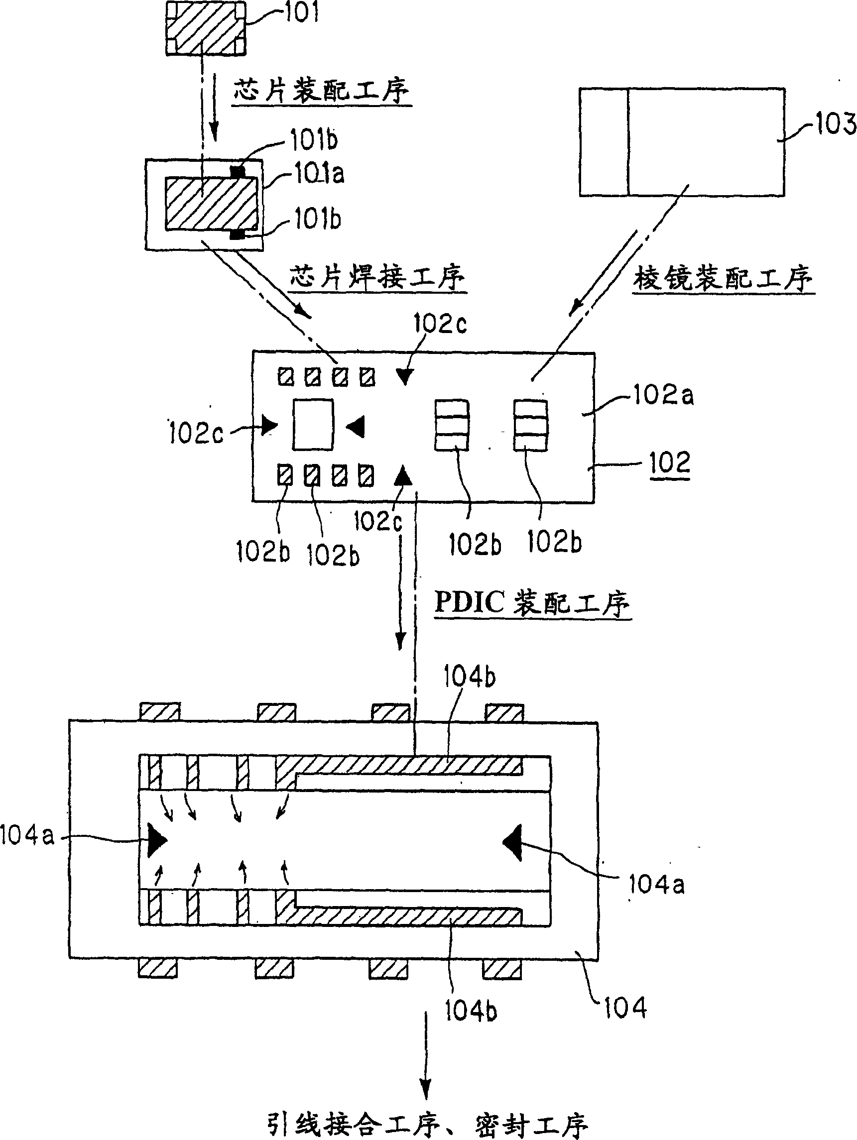
[0075] Embodiments of the present invention will be described below with reference to the drawings.

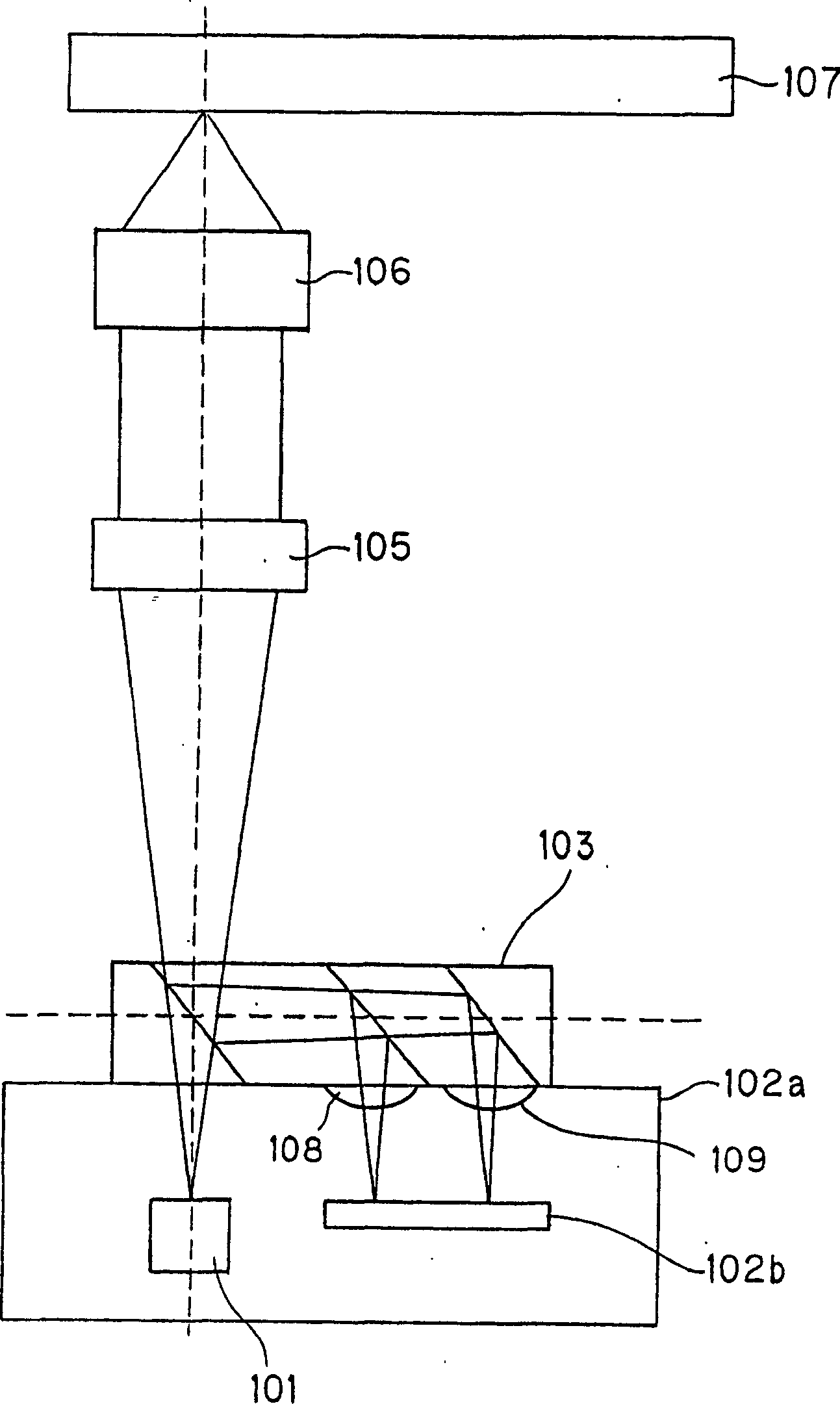
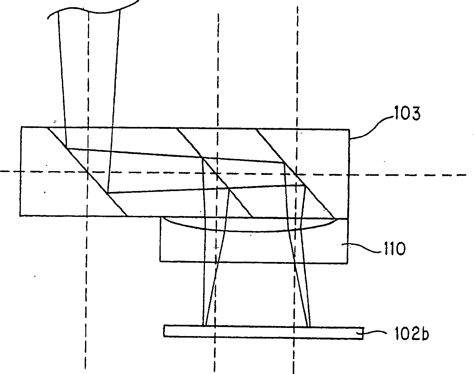
[0076] As shown in Figure 9, in the composite optical element and light receiving element device of the present invention, be provided with: be installed on one side of substrate 1 at least one optical element 2 that comprises lens, prism and diffractive element and be installed on substrate 1 On the other side, the semiconductor laser 3 and the light receiving element 4 as the light emitting element. Between the substrate 1 and the light receiving element 4, a relay substrate 5 as an intermediate member is provided. The manufacturing method of the composite optical element of this invention is a method for manufacturing such a composite optical element.

[0077] A first through hole 8 is formed on the substrate 1 to transmit the light beam emitted from the semiconductor laser 3 to one side of the substrate 1 . The substrate 1 is formed with a second through hole 9 through w...


PUM

PropertyMeasurementUnit
wavelengthaaaaaaaaaa

Abstract

The present invention concerns a hybrid optical element including at least one optical element (2) attached to one surface of a substrate (1), a semiconductor laser (3) and a photodetector (4) attached to the other surface of the substrate (1) and an intermediate member (relay substrate) (5) interposed between the substrate (1) and the photodetector (4). The intermediate member (5) has a through hole (6) through which a light flux incident on the photodetector (4) is allowed to pass and a part with a conductivity by which a terminals of the photodetector (4) are connected to a conductor pattern on the substrate (1).

Description

[0001] This application is a divisional application of the original application with the application number 02803245.4, the filing date of the original application is September 19, 2002, the earlier application is JP01-287564, and the priority date is September 20, 2001. technical field [0002] The present invention relates to a composite optical element and a light receiving element device of an optical head device for writing information signals on an optical recording medium such as an optical disk or reading information signals recorded on the optical recording medium. Background technique [0003] Conventional CDs (Compact Discs), so-called magneto-optical disks (MDs) with a diameter of 64 mm, and DVDs (Digital Versatile Discs: Digital Video Discs) have been used as recording media in recording and reproducing systems. , It is expected that the price will be lowered with the further miniaturization and weight reduction of the device. In order to meet such demands, it i...

Claims


Application Information

Patent Timeline
Patent Type & Authority Applications(China)
IPC IPC(8): G11B7/1369G11B7/22H01L31/12
CPCG11B7/135H01L31/12G11B7/13G11B7/22G11B7/1205G11B7/123G11B7/1369
Inventor 吉田浩谷口正小泽正文
Owner SONY GRP CORP
Features
  • R&D
  • Intellectual Property
  • Life Sciences
  • Materials
  • Tech Scout
  • Unparalleled Data Quality
  • Higher Quality Content
  • 60% Fewer Hallucinations
Learn More