
Array substrate for display device and display device

A technology for array substrates and display devices, applied to static indicators, instruments, etc., can solve problems such as increased switching times and increased load on signal line drive circuits

Inactive Publication Date: 2005-11-16
TOSHIBA MATSUSHITA DISPLAY TECH
View PDF1 Cites 3 Cited by
  • Summary
  • Abstract
  • Description
  • Claims
  • Application Information

AI Technical Summary

Problems solved by technology

Therefore, the number of times of switching increases, and the load on the signal line driver circuit increases.

Method used


Image

  • Array substrate for display device and display device
  • Array substrate for display device and display device
  • Array substrate for display device and display device

Examples


Embodiment 1

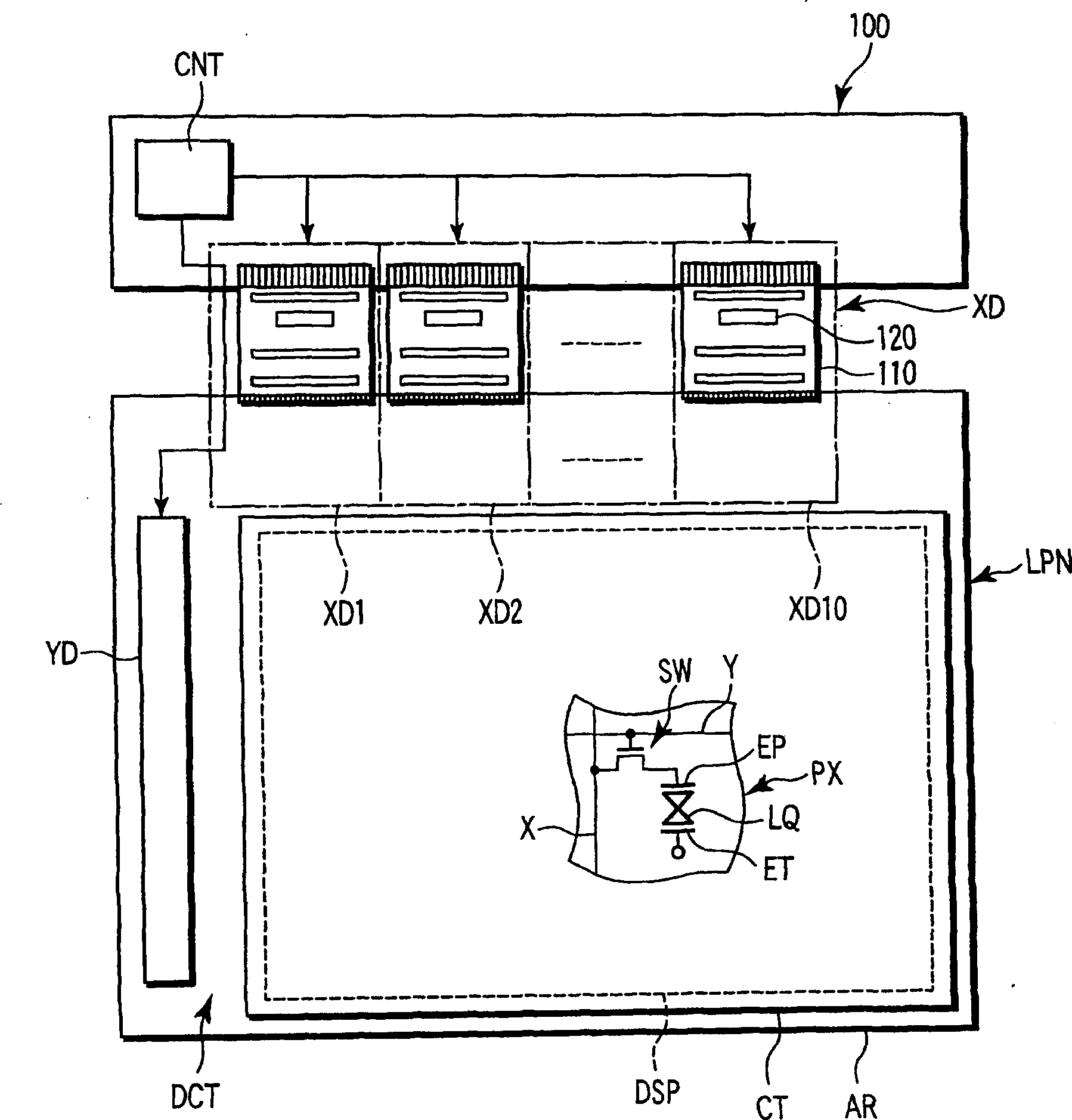
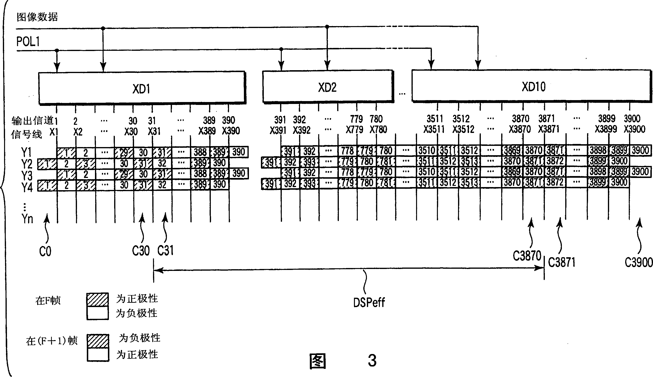
[0057] In this first embodiment, as shown in FIG. 3 , the signal line driving IC 120 has 3900 output channels, and the channels are used to output respective image signals to 3900 signal lines X1 to X3900, which are assigned as 390 A signal line consists of 10 area parts XD1-XD10.

[0058] In addition, the display area DSP has a substantially rectangular effective display portion DSP for displaying images. eff . That is, the effective display part DSP eff Defined as the fraction of pixel columns having m columns of n rows of pixels set. DSP in the adjacent effective display section eff On the outer side of the effective display portion of the pixel rows of the first column and the m-th column, dummy pixels that do not affect image display are provided as dummy pixel rows.

[0059] In the example shown in Figure 3, the effective display part DSP eff There are 3840 pixel columns from the 31st pixel column c31 to the 3870th pixel column c3870. In addition, 31 pixel columns ...

Embodiment 2

[0079] In the present embodiment 2, as shown in FIG. 5 , the signal line driving IC 120 has 3870 output channels, which are used to output image signals to 3870 signal lines X1 to X3870 respectively, and each 387 signal lines are distributed by Line one consists of 10 area parts XD1~XD10.

[0080] In the example shown in Figure 5, the effective display part DSP eff There are 3840 pixel columns from the first pixel column c1 to the 3840th pixel column c3840. In addition, the pixel column c0 of the 0th column adjacent to the pixel column c1 is set as a dummy pixel column. In addition, similarly, 30 pixel columns from the pixel column c3841 of the 3841st column adjacent to the pixel column c3840 to the pixel column c3870 of the 3870th column are also set as dummy pixel columns. In effective display part DSP eff The pixels on and the pixels on the dummy pixel column have substantially the same structure, and both contain switching elements.

[0081] The switching element of th...


PUM


Abstract

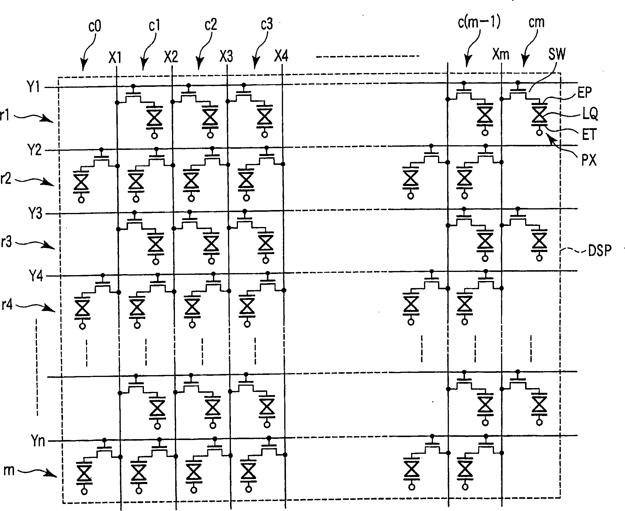
An array substrate includes m pixel columns in each of which n pixels PX are arranged in an effective display portion DSPeff, and dummy pixel columns obtained by arranging dummy pixels outside the effective display portion DSPeff. Each pixel and each dummy pixel include a switching element placed at the intersection of each scanning line and each signal line. One switching element is connected per row to each signal line. A switching element in the Nth row of the Mth pixel column and a switching element in the (N+1)th row of the (M+1)th pixel column are connected to the same signal line, and video signals having opposite polarities are supplied to adjacent signal lines.

Description

technical field [0001] The present invention relates to an array substrate for a display device and a display device, in particular to a structure of an array substrate constituting a display device such as a liquid crystal display device. Background technique [0002] In recent years, many flat-panel display devices represented by liquid crystal display devices adopt an active matrix driving method, that is, each pixel arranged in a matrix has a thin film transistor functioning as a switching element. In such a display device, there is a tendency that wiring impedance and wiring capacitance of wiring for transmitting signals such as images tends to increase in response to a demand for a larger screen size. Therefore, there occurs such a problem that the charging of each pixel is insufficient and the display quality deteriorates. For this reason, it is necessary to improve the capability of a signal line driver circuit for driving signal lines (that is, supplying a certain ...

Claims


Application Information

Patent Timeline
Patent Type & Authority Applications(China)
IPC IPC(8): G02F1/133G09G3/20G09G3/36
CPCG09G2300/0413G09G3/3648G09G3/3614G09G3/3607
Inventor 五十岚和明寺西谦太郎
Owner TOSHIBA MATSUSHITA DISPLAY TECH
Learn More