

Electronic device and its manufacturing method
A technology for electronic devices and manufacturing methods, applied in semiconductor/solid-state device manufacturing, circuits, electrical components, etc., can solve problems such as high leakage current, inability to form groove patterns, and photoresist residues.
- Summary
- Abstract
- Description
- Claims
- Application Information
AI Technical Summary
Problems solved by technology
Method used
Image

Examples
no. 1 example
[0123] Hereinafter, an electronic device and a manufacturing method thereof according to a first embodiment of the present invention will be described with reference to the drawings.
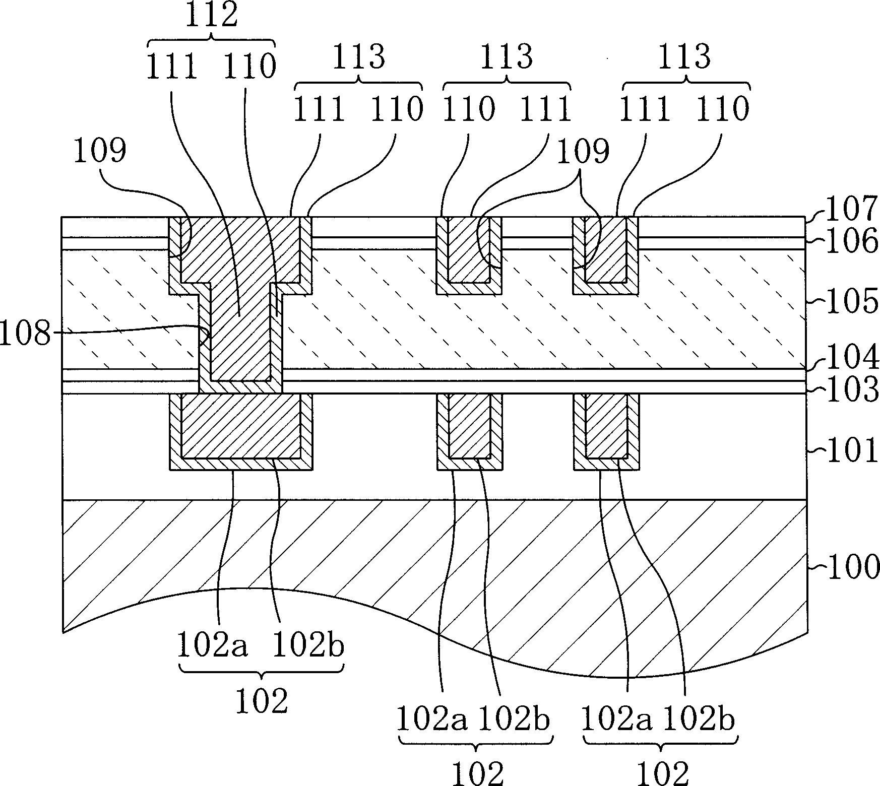
[0124] figure 1 , is a cross-sectional view showing the wiring structure of the electronic device according to the first embodiment of the present invention.
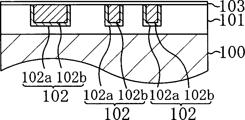
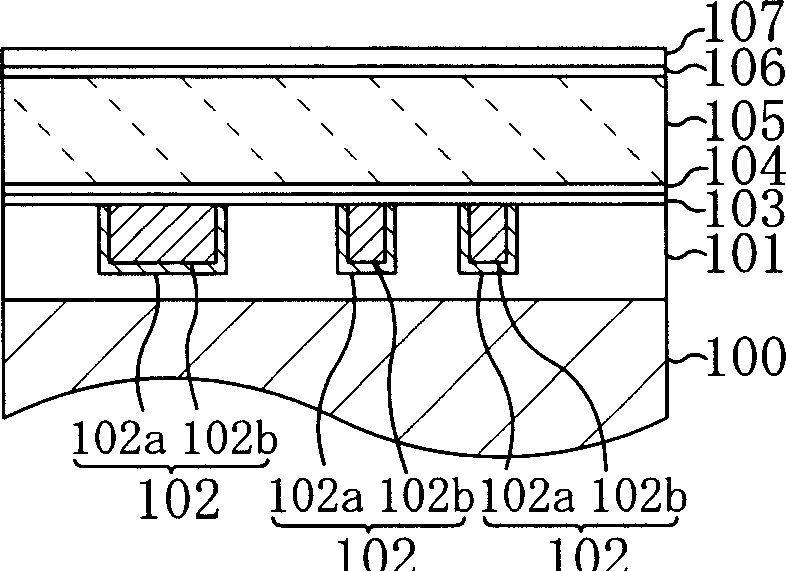
[0125] Such as figure 1 As shown, a lower layer metal wiring 102 is formed in a lower layer insulating film 101 formed on a substrate 100 made of, for example, silicon, and is composed of, for example, a tantalum nitride / tantalum laminate film 102a and a copper film 102b. A first nitrogen-containing insulating film 103 is formed on the lower layer metal wiring 102 and on the lower layer insulating film 101, and is formed of, for example, a silicon nitride carbide film. On the first nitrogen-containing insulating film 103 is formed a first nitrogen-free insulating film 104 made of, for example, a silicon oxide film. On the first nitro...
no. 1 approach
[0167] On the other hand, according to the first embodiment, by the following configuration (cf. figure 1 ): the first nitrogen-free insulating film 104 is sandwiched between the low dielectric constant film 105 and the first nitrogen-containing insulating film 103 on its underside, and the second nitrogen-containing insulating film 105 on the low dielectric constant film 105 and its upper side Interposing the second nitrogen-free insulating film 106 between the films 107 provides a remarkable effect of solving the problems of the comparative example described above.
no. 2 approach
[0169] Hereinafter, an electronic device and a manufacturing method thereof according to a second embodiment of the present invention will be described with reference to the drawings.
[0170] Figure 5 , is a cross-sectional view showing the wiring structure of the electronic device according to the second embodiment of the present invention.
[0171] Such as Figure 5 As shown, a lower layer metal wiring 202 is formed in a lower layer insulating film 201 formed on a substrate 200 made of, for example, silicon, and is composed of, for example, a tantalum nitride / tantalum laminate film 202a and a copper film 202b. On the lower layer metal wiring 202 and the lower layer insulating film 201 is formed a nitrogen-containing insulating film 203 made of, for example, a silicon nitride carbide film. On the nitrogen-containing insulating film 203 is formed a low dielectric constant film 204 made of, for example, a carbon-containing silicon oxide film. Formed on the low dielectric c...
PUM
 Abstract
Description
Claims
Application Information