Gas supply system and integrated unit for semiconductor manufacturing device

A technology for gas supply and manufacturing equipment, which is applied in semiconductor/solid-state device manufacturing, electrical components, and gases from chemical reactions, etc. It can solve problems such as pattern defects and deterioration of electrical characteristics, and achieve the effect of suppressing incorporation

Inactive Publication Date: 2008-09-03
TOKYO ELECTRON LTD
View PDF2 Cites 4 Cited by
  • Summary
  • Abstract
  • Description
  • Claims
  • Application Information

AI Technical Summary

Problems solved by technology

As the cause of device failure due to metal contamination, there are pattern defects caused by metallic contaminants (particles) at the particulate level, and deterioration of electrical characteristics caused by contaminants at the atomic or molecular level such as heavy metals, etc.

Method used


Image

  • Gas supply system and integrated unit for semiconductor manufacturing device
  • Gas supply system and integrated unit for semiconductor manufacturing device
  • Gas supply system and integrated unit for semiconductor manufacturing device

Examples


Embodiment Construction

[0025] Preferred embodiments of the present invention will be described in detail below with reference to the drawings. In addition, in this specification and drawings, the same code|symbol is attached|subjected to the component which has substantially the same functional structure, and repeated description is abbreviate|omitted.

[0026] (Structure Example of Semiconductor Manufacturing Equipment)

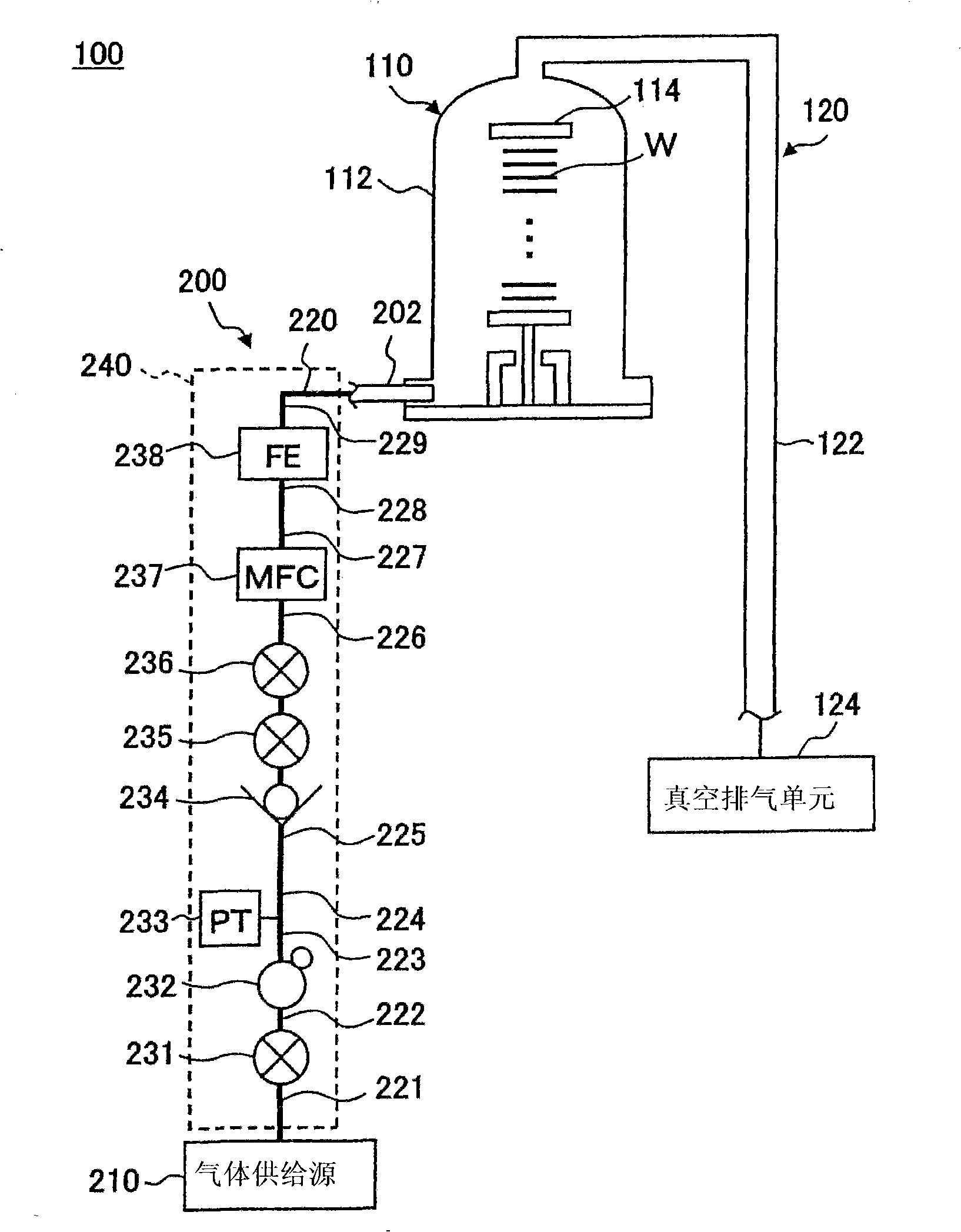
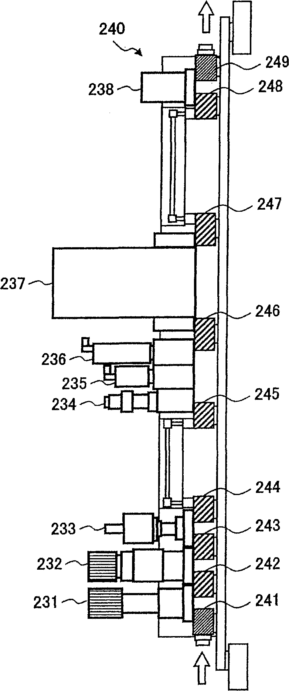
[0027] First, an embodiment in which the gas supply system of the present invention is applied to a semiconductor manufacturing apparatus will be described with reference to the drawings. Here, as a semiconductor manufacturing apparatus, a heat treatment apparatus for performing predetermined heat treatment on a substrate such as a semiconductor wafer (hereinafter also referred to simply as “wafer”) will be described as an example. figure 1 It is a figure which shows the structural example of the heat processing apparatus of this embodiment.

[0028] The heat treatment apparatus...


PUM


Abstract

The invention provides a gas supply system of a semiconductor manufacturing device and a gas supply integration unit. The gas supply system is used for supplying predetermined gas from a gas supply source to a processing part of a semiconductor manufacturing device. The gas supply system is provided with a gas supply flow path connected to the gas supply source and the processing part. The gas supply flow path comprises a plurality of fluid control devices (hand valve, reducing valve, manometer, check valve, first stop valve, second stop valve, quality flow controller and gas filter) and flow path components connected between the fluid control devices and forming gas flow paths. The flow path components are made of carbon material. Thereby, when corrosive gas is supplied to the processing part, mixing of metallic pollutants relative to a substrate to be processed may be inhibited.

Description

[0001] This patent application claims the priority of Japanese Patent Application No. 2007-045973 filed on February 26, 2007 as a Japanese application. The entire disclosure content of this prior application is incorporated by reference as a part of this specification. technical field [0002] The invention relates to a gas supply system and a gas supply integrated unit of a semiconductor manufacturing device. Background technique [0003] For example, a semiconductor manufacturing apparatus such as a diffusion apparatus, an etching apparatus, or a sputtering apparatus has a gas supply system for supplying gas from a processing gas supply source such as a gas cylinder to a processing unit. Then, by performing a process for manufacturing a semiconductor device using a gas supplied from the gas supply system, for example, a film forming process and an etching process using a predetermined gas, surface treatment is performed on a substrate to be processed such as a semiconducto...

Claims


Application Information

Patent Timeline
Patent Type & Authority Applications(China)
IPC IPC(8): H01L21/00C23C14/56C23C16/44C23F4/00C30B25/14H01J37/32
CPCC30B31/16C23C16/4402H01J37/3244Y02E60/34C23C16/45561C23C16/4404C30B25/14H01L21/20H01L21/22H01L21/306
Inventor 守谷修司中尾贤
Owner TOKYO ELECTRON LTD
Why Eureka
Try Eureka