Method for manufacturing ic card by laminating a plurality of foils

A manufacturing method and foil technology, which is applied in the field of IC card manufacturing, can solve problems such as COB falling off, insufficient electrical connection between the antenna connecting part and the COB electrode, and electrical connection interruption.

Inactive Publication Date: 2005-12-28
JT
View PDF0 Cites 6 Cited by
  • Summary
  • Abstract
  • Description
  • Claims
  • Application Information

AI Technical Summary

Problems solved by technology

[0004] However, there are following problems in the bonding of this method: that is, the electrical connection between the above-mentioned antenna connecting portion and the COB electrodes is not sufficient, and after using the IC card for a long time, the electrical connection will be interrupted, or the COB itself will fall off from the card.
In addition, in order to insert the COB into the groove formed on the laminated foil, the area of ​​the groove should be slightly larger than the area of ​​the COB structurally, so that there will be a gap between the above-mentioned COB and the groove of the completed IC card
Moisture may of course infiltrate through this gap, and when the card is deflected, the COB may also fall off the card board due to the above gap.

Method used


Image

  • Method for manufacturing ic card by laminating a plurality of foils
  • Method for manufacturing ic card by laminating a plurality of foils
  • Method for manufacturing ic card by laminating a plurality of foils

Examples


Embodiment Construction

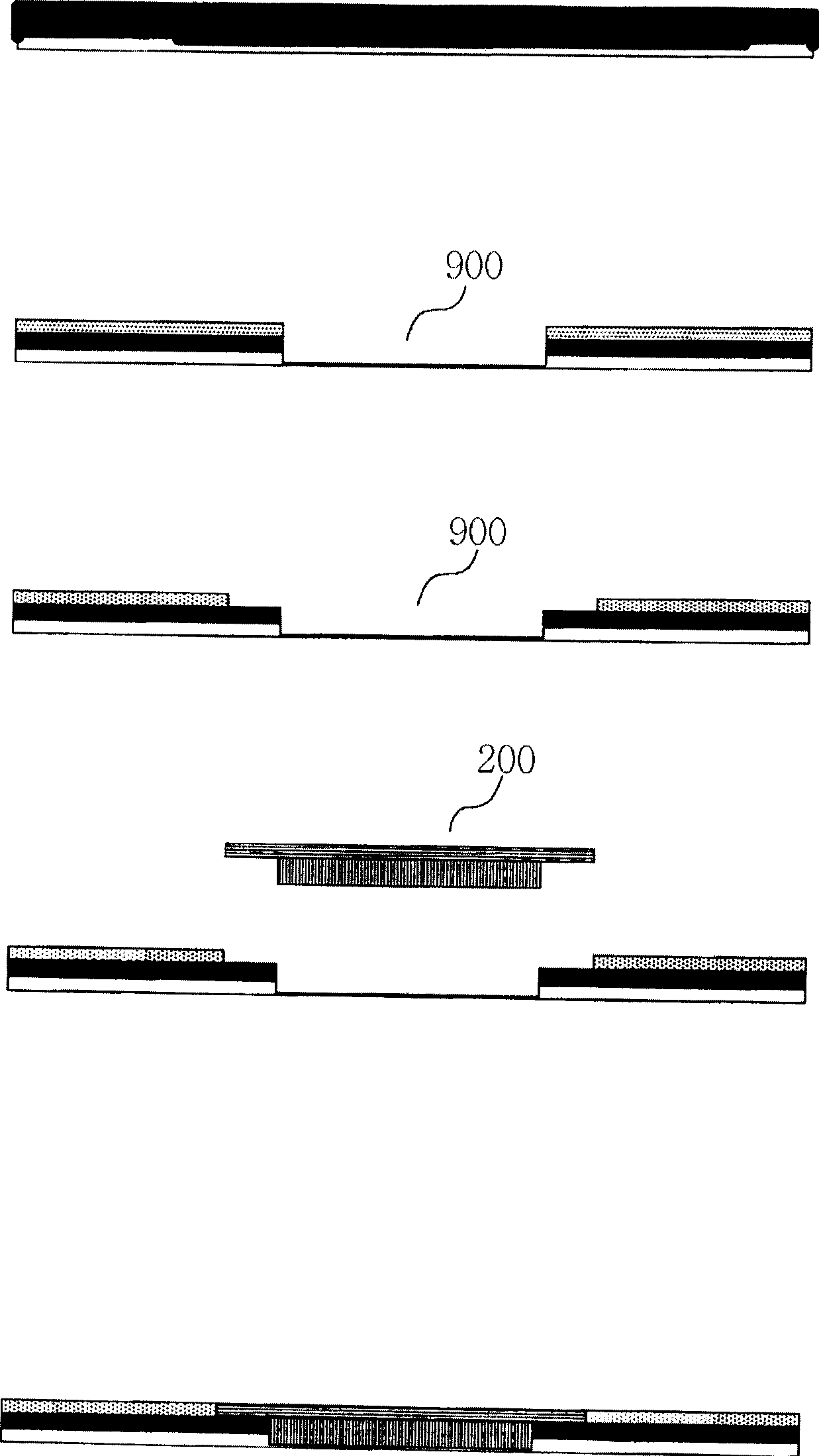
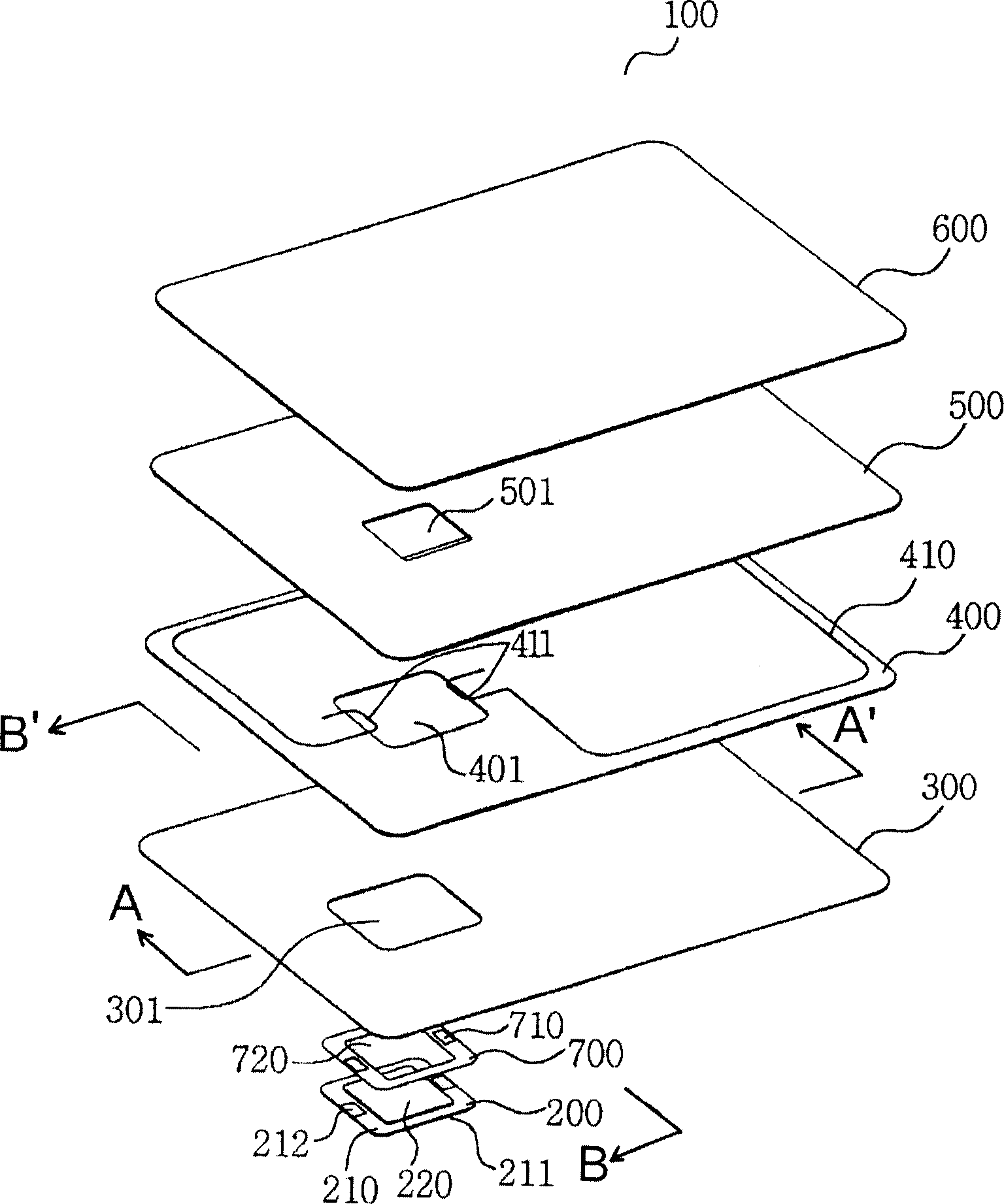
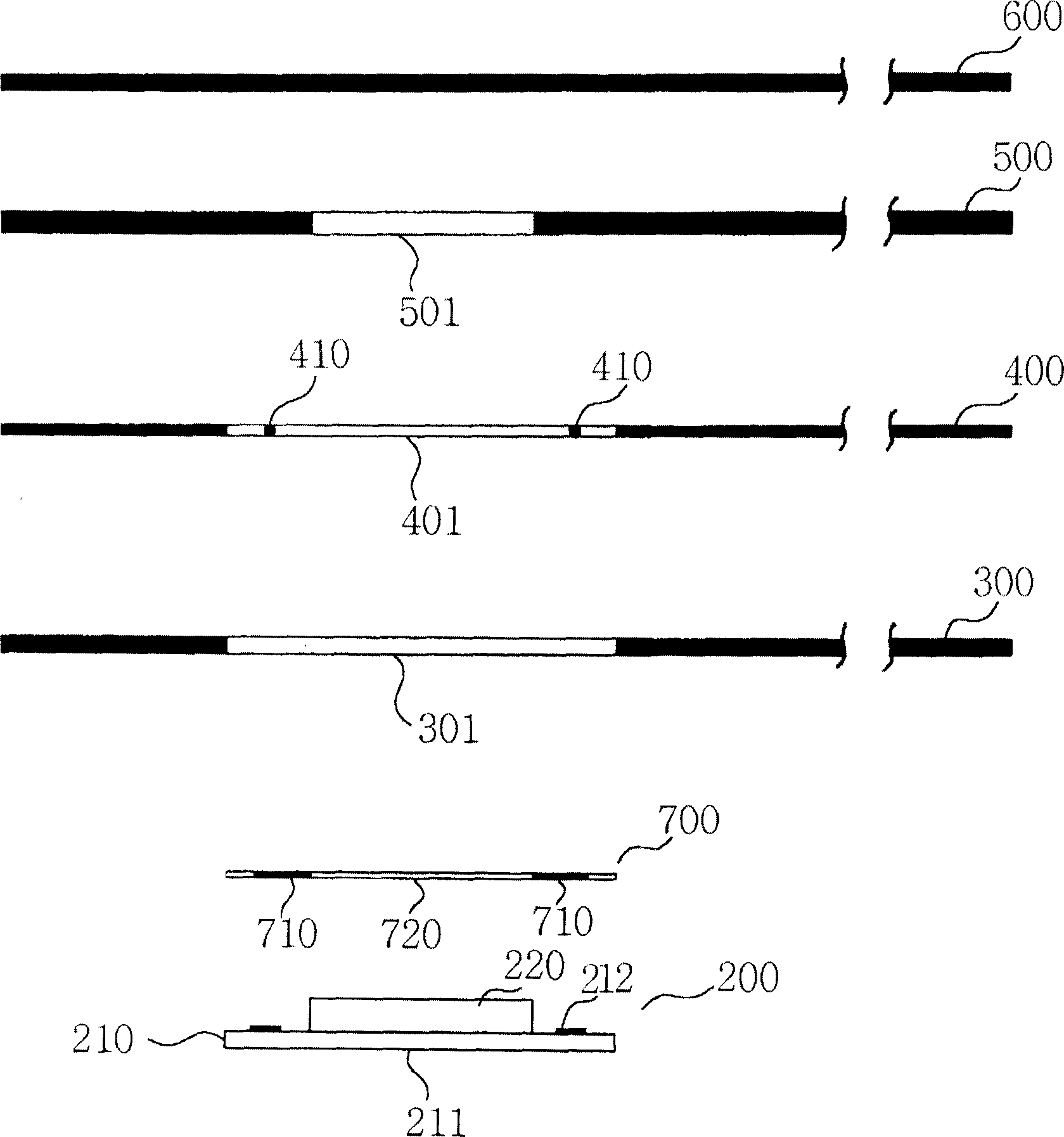
[0027]FIG. 2(A) is a perspective view illustrating a specific example of the IC card manufacturing process according to the present invention, and FIG. 2(B) is a sectional view thereof. The IC card (100) according to the present invention is formed by laminating a plurality of foils. First, a substantially flat working board (not shown) is placed on the bottom, and the COB ( 200 ) is placed on the working board. The working plate is preferably a metal plate having a certain thickness, which will be described below, and it has the advantage of being easy to heat and crimp the working plate. The above-mentioned COB (200) is a commonly used COB, and a chip chip is arranged on a main board (210), and a molding part (220) is formed thereon. The above molding part (220) does not only mean molding (moulding), but also can mean any purpose of protecting the above chip including potting. In this kind of COB (200), for the COB (200) used for contact cards, the lower side of the main b...


PUM


Abstract

PURPOSE: A method for manufacturing an IC card by layering foils is provided to remove a step for digging out a groove again after layering the foils, firmly join the COB(Chip On Board) and a card plate, occur no gap between the COB and the card plate, and firmly join an electrode of the COB and an antenna. CONSTITUTION: The COB(200) is placed by facing an electrode surface of a terminal in the COB downwardly. At least more than two foils(300,400,500) having a hole(301) of the same area as the COB are layered by inserting the COB into the hole. A back side cover foil(600) having no hole is layered to an opposite side of the surface exposing the electrode surface of the terminal in the COB of the layered foils, and the foils are compressed.

Description

field of invention [0001] The invention relates to an IC card manufacturing method. More specifically, the present invention relates to a method of manufacturing an IC card by laminating at least two foil sheets formed with holes corresponding to COB (Chip On Board) and bonding them to each other by pressure. Background technique [0002] IC cards, which are cards carrying necessary data and programs in COB, are being used in more and more fields because of their convenience and good information retention capabilities. This kind of IC card can generally be divided into: through the contact between the card reader terminal and the electrode, the contact IC card that realizes the input and output of information, has an antenna inside, even if it is not in contact with the card reader terminal, A non-contact IC card capable of inputting and outputting information, and a combined IC card capable of realizing the functions of the above-mentioned contact and non-contact IC cards....

Claims


Application Information

Patent Timeline
Patent Type & Authority Applications(China)
IPC IPC(8): G06K19/077
CPCG06K19/07722G06K19/07745
Inventor 柳弘俊金正镐
Owner JT
Why Eureka
Try Eureka