Eureka AIR delivers breakthrough ideas for toughest innovation challenges, trusted by R&D personnel around the world.

Manufacturing method for semiconductor chips

一种制造方法、半导体的技术,应用在半导体/固态器件制造、半导体器件、电固体器件等方向,能够解决不能避免碎屑等问题,达到改善横向破裂强度的效果

Active Publication Date: 2008-04-09
PANASONIC CORP
View PDF2 Cites 3 Cited by
  • Summary
  • Abstract
  • Description
  • Claims
  • Application Information

AI Technical Summary

Problems solved by technology

There is a problem that when the sharp corner portion 554 is formed on the semiconductor chip as described above, generation of chipping cannot be avoided

Method used


Image

  • Manufacturing method for semiconductor chips
  • Manufacturing method for semiconductor chips
  • Manufacturing method for semiconductor chips

Examples


no. 1 example

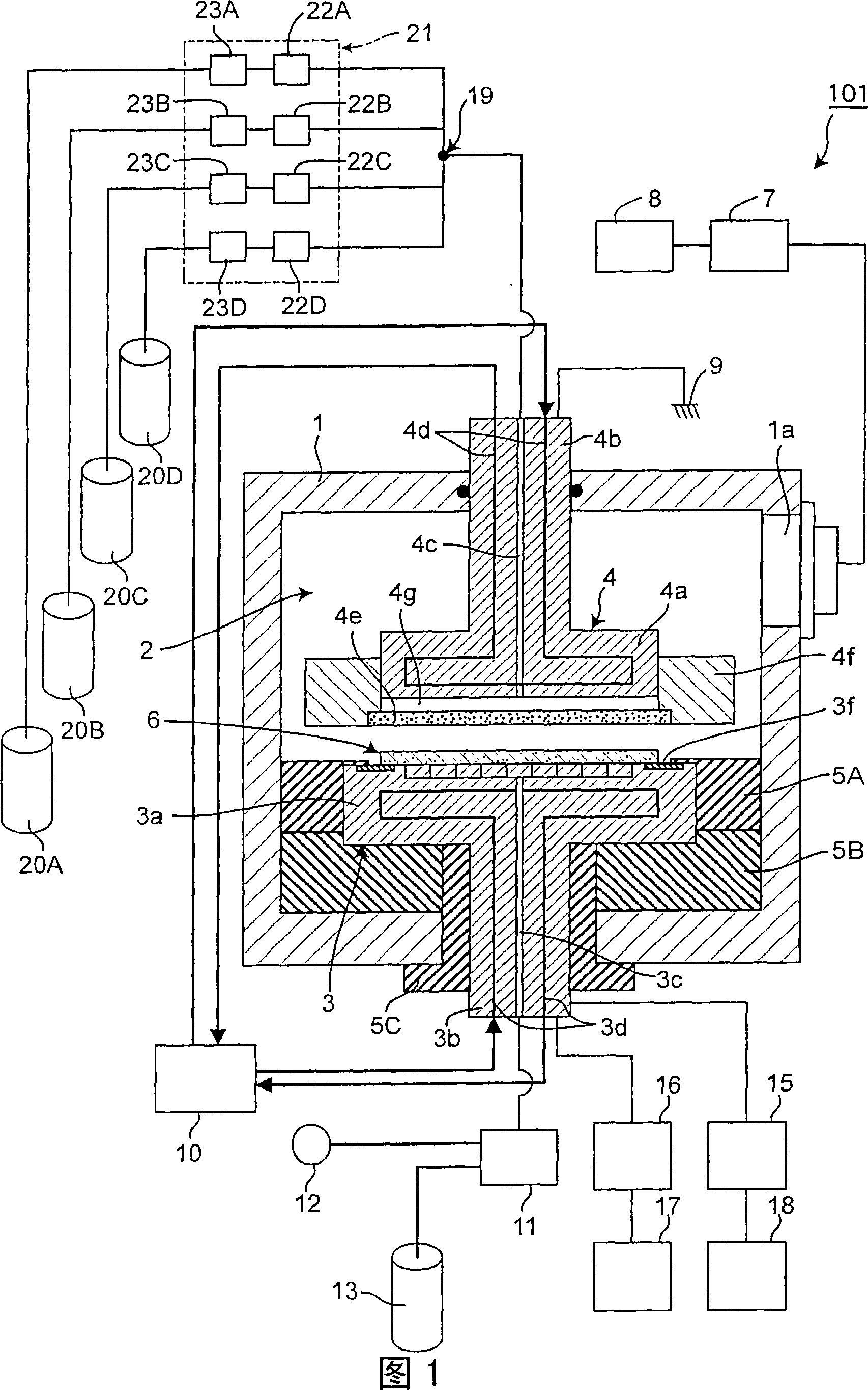
[0142] Structure of plasma processing equipment

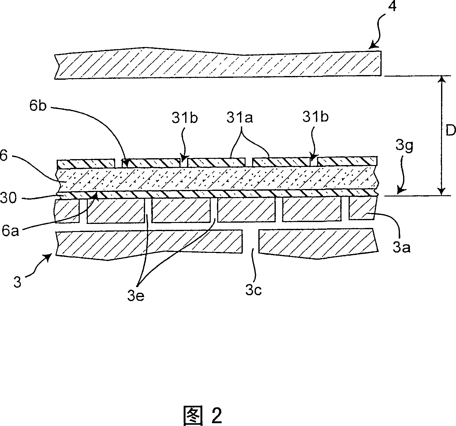
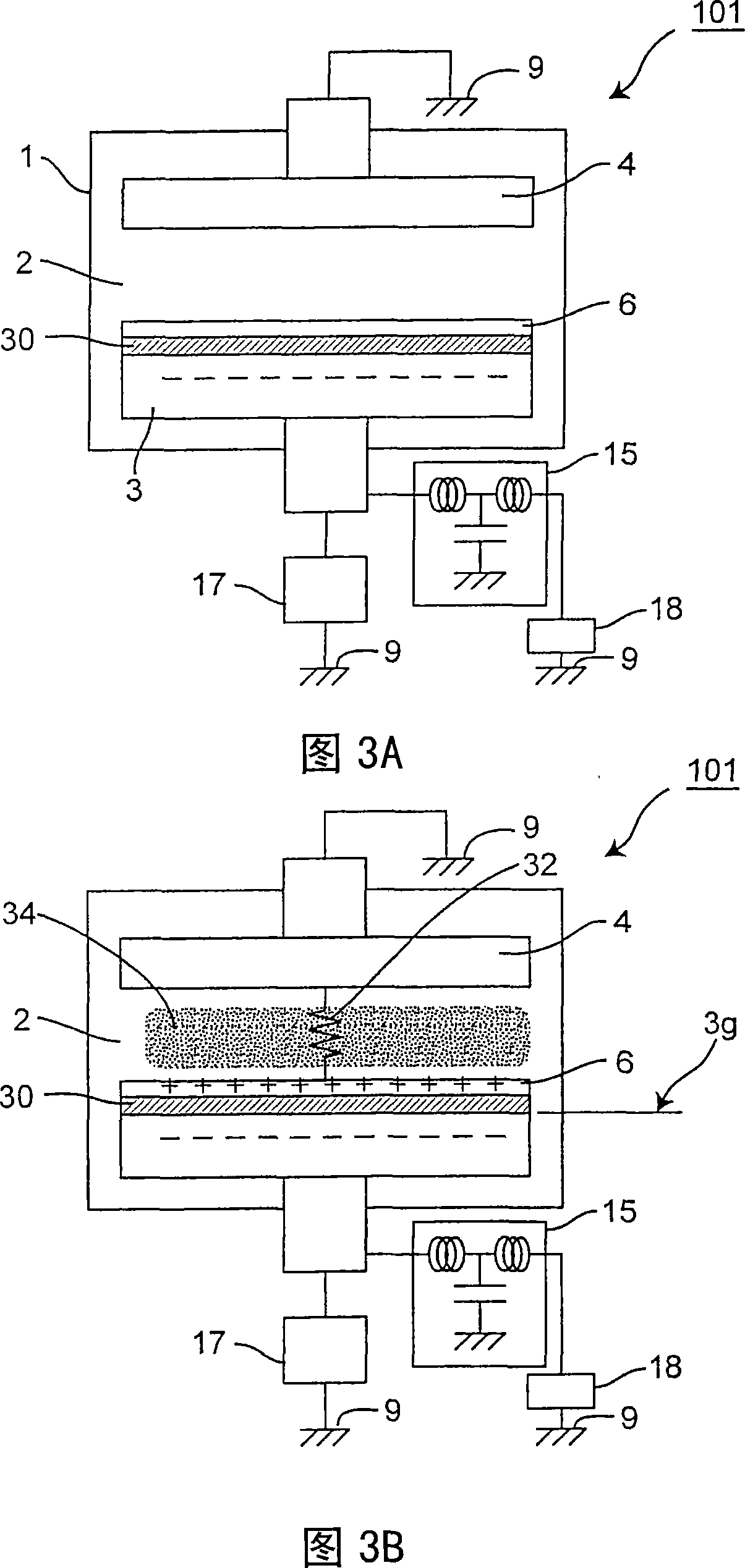
[0143] FIG. 1 shows a schematic structural view schematically showing the structure of a plasma processing apparatus for dividing a semiconductor wafer by a method of manufacturing a semiconductor chip according to a first embodiment of the present invention. It should be noted that FIG. 1 is a longitudinal sectional view showing a plasma processing apparatus 101 . The plasma processing apparatus 101 is an apparatus that manufactures semiconductor chips by dividing a semiconductor wafer into individual pieces of semiconductor chips including semiconductor devices on a circuit formation surface (first surface) on which a plurality of semiconductors are formed.

[0144] In the sequence of the semiconductor manufacturing process as described above, a protective sheet made of a material that is more difficult to etch than silicon, which is the basic material of the semiconductor wafer, is pasted on the circuit formation surface o...

no. 2 example

[0243] The present invention is not limited to the above embodiments, but allows implementation in various modes. For example, a method of manufacturing a semiconductor chip according to a second embodiment of the present invention is described below with reference to schematic exemplary views shown in FIGS. 16A to 16C , FIGS. 17A to 17C , FIGS.

[0244] The semiconductor chip manufacturing method of this second embodiment differs from the first embodiment in that a polyimide (PI) film is used as an insulating film instead of using the silicon oxide film 35 as in the semiconductor wafer 6 of the first embodiment. As an insulating film formed in a portion corresponding to the divided region R2. Only the differences are described below. The fact that the plasma processing apparatus used in the first embodiment is similarly used by the semiconductor chip manufacturing method of this second embodiment is the same, and therefore a description for the apparatus is not provided. In...

no. 3 example

[0261] Next, it will be described with reference to the flow chart of the program shown in FIG. 22 and the schematic exemplary diagrams shown in FIGS. 23A to 23C, FIGS. 24A to 24C, FIGS. 25A and 25B, and FIGS. A method of manufacturing a semiconductor chip according to a third embodiment of the present invention. With the method of manufacturing a semiconductor chip of this third embodiment, notch formation and the like are performed by using a protective sheet having an insulating property as an insulating film placed in a division different from that of the first and second embodiments. in zone R2. Only the differences are described below. Furthermore, the manufacturing method of the semiconductor chip of the third embodiment can be performed by the processing device 101 used in the first embodiment. Therefore, a description of the structure and the like of the plasma processing apparatus 101 will not be provided.

[0262]As shown in FIG. 23A , a semiconductor device 344 ...


PUM


Abstract

By performing plasma etching on the second surface of a semiconductor wafer on the first surface of which an insulating film is placed in dividing regions and on the second surface of which a mask for defining the dividing regions are placed, the second surface being located opposite from the first surface, the insulating film is exposed from an etching bottom portion by removing portions that correspond to the dividing regions. Subsequently, by continuously performing the plasma etching in the state in which the exposed surfaces of the insulating film are charged with electric charge due to ions in the plasma, corner portions put in contact with the insulating film are removed. Subsequently, by removing the mask and thereafter performing plasma etching on the second surface, corner portions located on the second surface side are removed.

Description

technical field [0001] The present invention relates to a semiconductor chip manufacturing method for forming semiconductor devices arranged in a plurality of device formation regions by dividing regions on a first surface of a semiconductor wafer and individually separating device formation regions of the semiconductor wafer along the divided regions The plurality of device formation regions are defined, thereby manufacturing a semiconductor chip including individualized semiconductor devices. Background technique [0002] Generally, as a method of dividing a semiconductor chip into individual semiconductor chips by such a manufacturing method of a semiconductor chip, various methods have been known. For example, a method for dividing a semiconductor wafer by mechanically dicing the wafer by a rotating blade called a dicing blade. [0003] However, in recent years, the wafers of the present invention have become thinner and thinner, and when a semiconductor wafer vulnerabl...

Claims


Application Information

Patent Timeline
Patent Type & Authority Applications(China)
IPC IPC(8): H01L21/78H01L21/68H01L21/3065
CPCH01L21/6835H01L2221/6834H01L21/3065H01L21/78H01L2221/68354H01L2924/30105H01L21/30H01L21/68
Inventor 有田洁中川显
Owner PANASONIC CORP
Why Eureka
Eureka Blog
Learn More