Semiconductor device and process for producing the same

A manufacturing method and semiconductor technology, applied in the direction of semiconductor/solid-state device manufacturing, semiconductor devices, semiconductor/solid-state device components, etc., can solve the problem that the bumps are not in contact with each other and the insulating resin layer cannot prevent the metal bumps from being damaged. Alignment etc.

Inactive Publication Date: 2006-01-18
SONY CORP
View PDF1 Cites 7 Cited by
  • Summary
  • Abstract
  • Description
  • Claims
  • Application Information

AI Technical Summary

Problems solved by technology

Therefore, the opening of the insulating resin layer cannot function to prevent misalignment with the metal bump
Furthermore, in the manufacturing method described in the above Patent Document 1, the bumps are not bonded in contact with each other
Therefore, the manufacturing method described in the above Patent Document 1 cannot solve the problem to be solved by the present invention, that is, when the semiconductor chip 1 is mounted on the mounting substrate 3 by flip-chip bonding as described above, the bumps Joint failure caused by misalignment between 2 and 4

Method used


Image

  • Semiconductor device and process for producing the same
  • Semiconductor device and process for producing the same
  • Semiconductor device and process for producing the same

Examples


Embodiment Construction

[0019] Hereinafter, embodiments of the present invention will be described in detail with reference to the drawings.

[0020] In the semiconductor device manufacturing method according to the present invention, flip chip bonding in which the electrodes of the semiconductor chip and the mounting substrate are electrically connected through bonding bumps are used to mount the semiconductor chip on the mounting substrate. The specific process of this method will be described below.

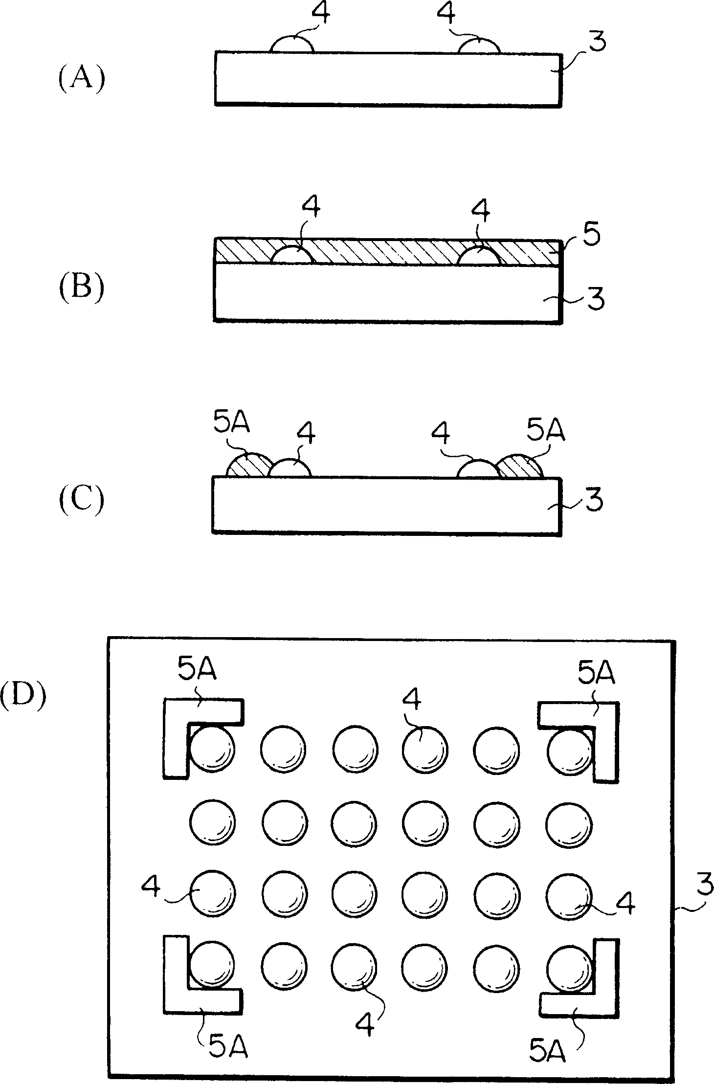
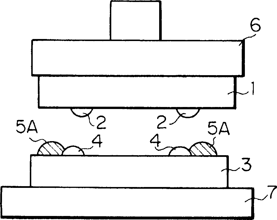
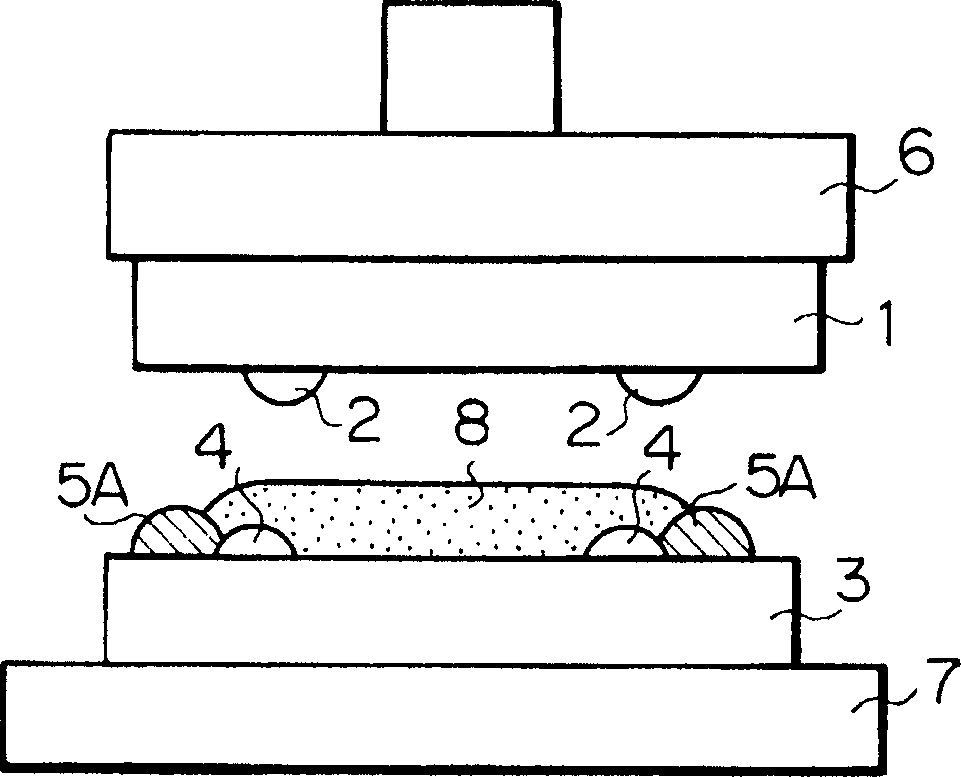
[0021] Figure 1 to 3B It is an explanatory diagram showing a specific example of a method of manufacturing a semiconductor device according to an embodiment of the present invention. In the description of this embodiment, components similar to those in the above-mentioned conventional technology are denoted by the same reference numerals.

[0022] First, like figure 1 As shown in (A), a plurality of bumps 4 are formed on the chip mounting surface of the mounting substrate 3 on which the semiconductor ...


PUM


Abstract

When a semiconductor chip is mounted on a mount substrate by bonding bumps, bonding failure is caused by misalignment between the bumps. <??>Before a semiconductor chip having a plurality of bumps is mounted on a mount substrate (3) having a plurality of bumps (4) by flip chip bonding, a resist layer (5) having a thickness larger than that of the bumps (4) is formed on the mount substrate (3) with the bumps. By patterning the resist layer (5), projecting guides (5A) of semicircular cross section are formed on the mount substrate (3) so as to protrude near the bumps (4) and from a surface on which the bumps (4) are provided, and to have guide faces (curved faces) pointing toward the bumps (4).

Description

Technical field [0001] The present invention relates to a manufacturing method of a semiconductor device and a semiconductor device manufactured by the manufacturing method, and the method is suitable for mounting a semiconductor chip on a mounting substrate through bonding bumps. Background technique [0002] Currently, SIP (System Package) obtained by combining multiple LSI (Large Scale Integration) devices such as CPU (Central Processing Unit) and memory into one package has been considered as a package for high-performance semiconductor devices Types of. Some SIPs adopt a package form in which multiple semiconductor chips are mounted on a common mounting substrate (interposer). Some other SIPs use semiconductor chips with a diameter larger than the diameter of the semiconductor chip to be mounted on them as the mounting substrate, that is, chip-on-chip SIPs. [0003] As a method of mounting semiconductor devices by using such a SIP package form, flip-chip bonding has recently...

Claims


Application Information

Patent Timeline
Patent Type & Authority Applications(China)
IPC IPC(8): H01L21/60H05K3/34H01L21/56H01L23/498H05K3/30
CPCH01L2224/73203H01L2924/01027H01L24/29H05K3/303H01L2224/81801H01L24/32H01L2924/01039H01L2924/12044H01L2924/01015H01L2924/0105H01L2224/83051H01L2224/16225H01L2224/10165H01L2924/01004H01L2924/01078H01L2224/27013H01L2924/01006H01L23/49811H01L2924/01079H01L2224/83192H01L2924/01005H01L2924/01082H01L2224/73204H01L21/563H05K2201/09909H01L2924/01013H01L2224/73103H01L2224/81136H01L2924/014H05K2201/10674H01L2224/8114H01L2924/01018H01L2224/16145H05K2203/167H01L2924/01019H01L2924/01033H01L2924/01068H01L24/81H01L2224/73104H01L2224/16105H01L2224/81193H01L2224/81194Y02P70/50
Inventor 仙田亚由美
Owner SONY CORP
Why Eureka
Try Eureka