Fast response broad band laser detector made by oxide heterojunction material
A technology of laser detectors and heterojunctions, applied in the field of laser detectors, can solve the problems that the response band is not wide enough, the photoresponse of detectors is not fast enough, and it cannot be used to detect and measure laser pulse pulse laser waveforms, etc., and achieves the preparation method Simple, high-sensitivity effects
- Summary
- Abstract
- Description
- Claims
- Application Information
AI Technical Summary
Problems solved by technology
Method used
Image
Examples
Embodiment 1
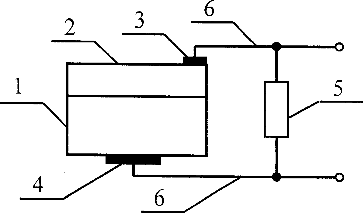
[0022] refer to figure 1 , to prepare a laser detector with a two-layer structure of doped strontium niobate titanate-doped lanthanum manganate. The following is combined with the specific preparation process to describe in detail the structure of the fast-response broadband laser detector made of oxide heterojunction materials in the present invention. To explain:
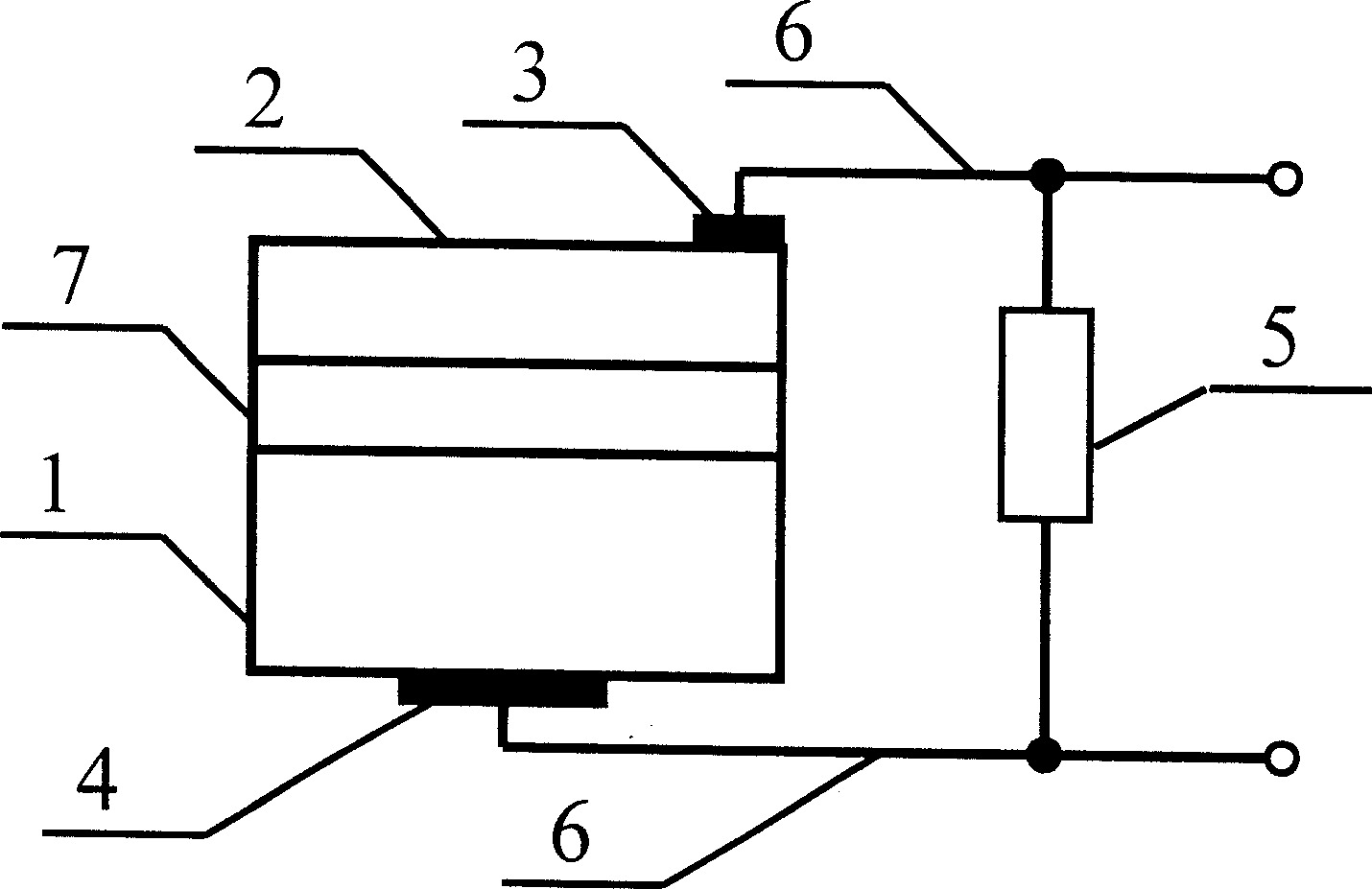
[0023] Laser molecular beam epitaxy equipment is selected, and the substrate is 1×1cm 2 SrNb 0.01 Ti 0.99 o 3 Doped strontium niobate titanate 1, on which a 300nm thick La 0.7 Sr 0.3 MnO 3 Photoresponsive material layer 2, forming La 0.7 Sr 0.3 MnO 3 / SrNb 0.01 Ti 0.99 o 3 Two-layer oxide heterostructure sample, with 1×0.5cm 2 La 0.7 Sr 0.3 MnO 3 / SrNb 0.01 Ti 0.99 o 3 The sample is used as the detector core; the second electrode 4 of about φ2mm is welded on the surface of strontium niobate titanate doped with indium, and the second electrode 4 of about φ2mm is welded on the surface of La 0.7 S...
Embodiment 2
[0027] Using laser molecular beam epitaxy equipment, on SrNb with a diameter of φ25mm 0.1 Ti 0.9 o 3 Direct epitaxial growth of 100 nm thick La on substrate 1 0.7 Sr 0.3 MnO 3 Thin film photoresponsive material layer 2, prepared La 0.7 Sr 0.3 MnO 3 / SrNb 0.1 Ti 0.9 o 3 The two-layer heterostructure sample was used as a chip, and a sample with a diameter of φ25mm was used as a chip, and the chip was deposited on La by magnetron sputtering. 0.7 Sr 0.3 MnO 3 The outer circle of the thin film 2 prepares a silver electrode 3 with a width of 0.5mm, SrNb 0.1 Ti 0.9 o 3 A circular silver electrode 4 with a diameter of 10 mm is prepared in the center of the substrate 1, and the assembly is the same as that of the laser detector with a two-layer structure prepared in Example 1.
Embodiment 3
[0029] Select laser molecular beam epitaxy device for use, make according to embodiment 1, in 1 * 1cm 2 SrNb 0.005 Ti 0.995 o 3 800nm thick La was epitaxially grown on substrate 1 0.95 Ba 0.05 MnO 3 Thin film photoresponsive material layer 2, forming La 0.95 Ba 0.05 MnO 3 / SrNb 0.005 Ti 0.995 o 3 Two-layer heterostructure chip, in La 0.95 Ba 0.05 MnO 3 One edge of the thin film layer is vacuum-evaporated with a 0.5mm wide platinum first electrode 3, and the rest is the same as the structure of the fast-response broadband laser detector made of oxide heterojunction materials prepared according to Example 1.
PUM
 Abstract
Description
Claims
Application Information


