

Semiconductor device with improved breakdown voltage and high current capacity
A semiconductor and component technology, applied in the field of vertical power semiconductor components, can solve problems such as destroying components, and achieve the effects of improving avalanche current, high withstand voltage, and improving avalanche destruction current
- Summary
- Abstract
- Description
- Claims
- Application Information
AI Technical Summary
Problems solved by technology
Method used
Image

Examples
Embodiment approach 1
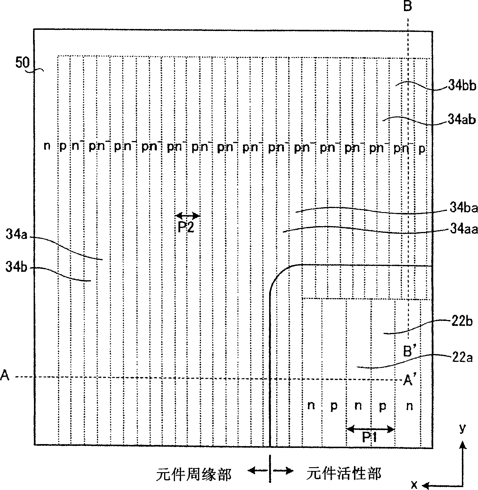
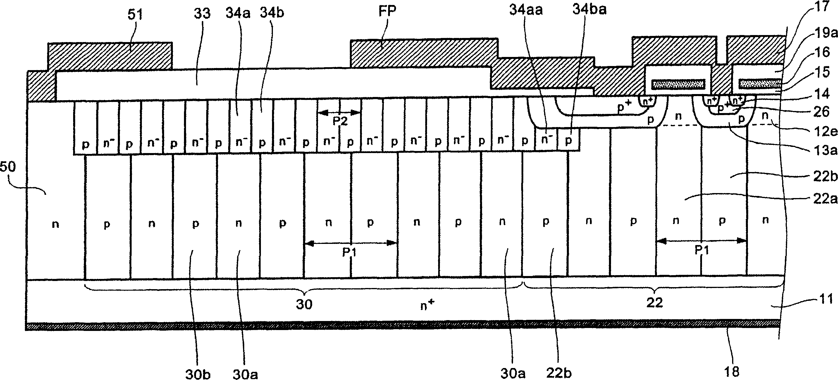
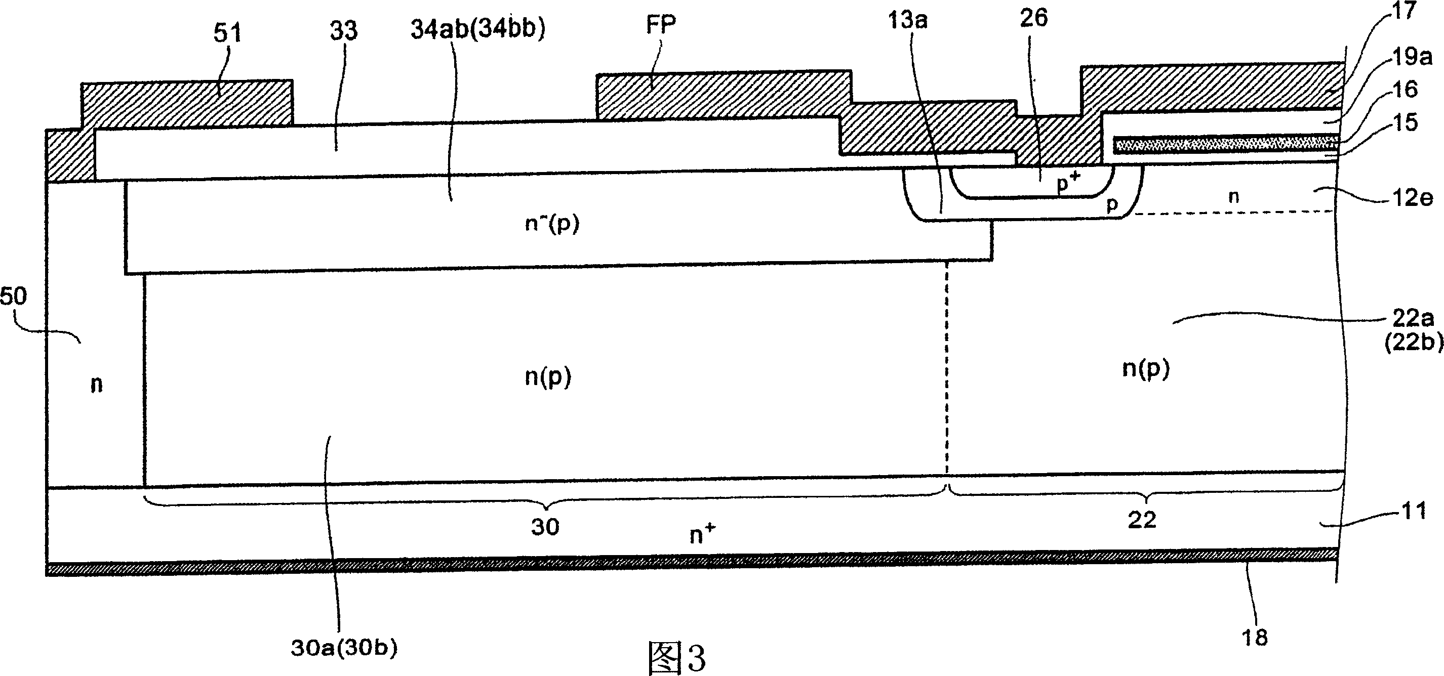
[0126] figure 1 is a schematic partial plan view showing a chip of a vertical MOSFET element according to Embodiment 1 of the present invention, figure 2 is to mean along figure 1 A vertical cross-sectional view of the state cut along the line A-A' in Fig. 3 is a representation along the figure 1 In the vertical cross-sectional view of the state cut by the BB' line, in the vertical MOSFET of Embodiment 1, except that the impurity concentration of the third p-type regions 34b, 34ba, 34bb is higher than the impurity concentration of the third n-type regions 34a, 34aa, 34ab Besides, with Figure 23 ~ Figure 2 The conventional configuration shown in 5 is the same.
[0127] Such as figure 1 As shown, in Embodiment 1, the first parallel pn structure, the second parallel pn structure, and the third parallel pn structure are arranged parallel to each other in a planar stripe shape. In the third side-by-side pn configuration, the widths of the third n-type regions 34a, 34aa, ...
Embodiment approach 2
[0140] Figure 7 is a schematic partial plan view showing a chip of a vertical MOSFET element according to Embodiment 2 of the present invention, Figure 8 is to mean along Figure 7 A longitudinal sectional view of the state cut by the line A-A' in Figure 9 is to mean along Figure 7 A vertical cross-sectional view of the state where B-B' in is cut. The vertical MOSFET of Embodiment 2 is a modified example of Embodiment 1, and differs from Embodiment 1 in the following points. That is, the impurity concentrations of the third n-type region 34a and the third p-type region 34b are the same, and the width Wp of the third p-type region 34b is wider than the width Wn of the third n-type region 34a. For example, the impurity concentrations of the third n-type region 34a and the third p-type region 34b are 4.8×10 14 cm -3 The width Wp of the third p-type region 34b is 120% or more of the width of the third n-type region 34a.
[0141] In addition, the direction of the repetit...
Embodiment approach 3
[0144] Figure 10 It is a schematic partial plan view showing a chip of a vertical MOSFET element according to Embodiment 3 of the present invention. Figure 11 is to mean along Figure 10 A vertical cross-sectional view of the state where the line A-A' is cut. The vertical MOSFET of Embodiment 3 is a modified example of Embodiment 2, and differs from Embodiment 2 in the following points. That is, the p-type regions 22b', 30b', 34b' and n-type regions 22a', 30a', 34a' of the first to third parallel pn structures are vertically layered, not planar stripes, and the p-type regions 22b ', 30b', 34b' are planar hexagonal lattice points, and the remaining parts become n-type regions 22a', 30a', 34a'. Conversely, the n-type region may be in the form of hexagonal lattice points, and the remaining part may be a p-type region.
[0145] In addition, if the impurity amount of the third p-type region 34b' is larger than the impurity amount of the third n-type region 34a' in the third p...
PUM
 Abstract
Description
Claims
Application Information