SOI-based gate-controlled lateral SAM structure blue-violet light single-photon detector and its preparation method

A single-photon detector and gate-controlled technology, applied in the field of blue-violet light single-photon detection, can solve the problems of small input impedance, long dead time, unfavorable integration, etc., and achieve the effects of large input impedance, accelerated recovery, and reduced dark current.

Active Publication Date: 2019-11-15
CHANGSHA UNIVERSITY OF SCIENCE AND TECHNOLOGY
View PDF6 Cites 0 Cited by
  • Summary
  • Abstract
  • Description
  • Claims
  • Application Information

AI Technical Summary

Problems solved by technology

Therefore, the dead time is long
In addition, the existing single-photon detectors are usually bipolar structures based on longitudinal PN junctions, the quantum efficiency and frequency response are mutually restricted, and the input impedance is small, which is not conducive to integration

Method used


Image

  • SOI-based gate-controlled lateral SAM structure blue-violet light single-photon detector and its preparation method
  • SOI-based gate-controlled lateral SAM structure blue-violet light single-photon detector and its preparation method
  • SOI-based gate-controlled lateral SAM structure blue-violet light single-photon detector and its preparation method

Examples


Embodiment Construction

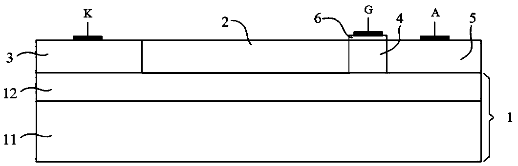
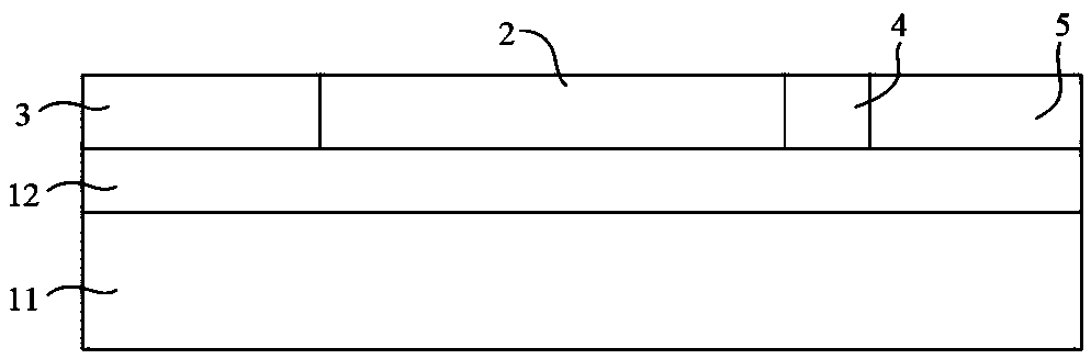
[0025] Such as figure 1 As shown, the SOI-based gate-controlled lateral SAM structure blue-violet single-photon detector of this embodiment includes a surface with P - type silicon thin film 2 on SOI substrate 1, P - The thickness of type silicon thin film 2 is 100nm~800nm, P - One side of type silicon thin film 2 is provided with P + Zone 3, the other side is provided with adjacently arranged P zones 4 and N + District 5, P + The surface of the region 3 is provided with an electrode K, the surface of the P region 4 is provided with a gate oxide layer 6, and the surface of the gate oxide layer 6 is provided with gate electrodes G, N + The surface of zone 5 is provided with electrodes A.

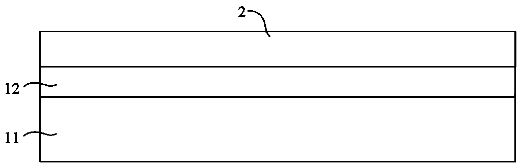
[0026] Such as figure 1 As shown, in this embodiment, the SOI substrate 1 includes stacked P - Substrate 11 and SiO 2 Layer 12, P - type silicon thin film 2 set on SiO 2 layer 12 surface.

[0027] In this example, P - The thickness of the substrate 11 is 500 nm.

[0028] In this ...


PUM


Abstract

The invention discloses an SOI-based gate-controlled transverse SAM structured blue purple light single-photon detector and a preparation method thereof. The blue purple light single-photon detector comprises an SOI substrate with a P- type silicon thin film on the surface; a P+ region is arranged on one side of the P- type silicon thin film while a P region and an N+ region which are arranged adjacently are arranged on the other side; an electrode K is arranged on the surface of the P+ region; a gate oxide layer is arranged on the surface of the P region; a gate electrode G is arranged on thesurface of the gate oxide layer; and an electrode A is arranged on the surface of the N+ region. The preparation method comprises the steps of generating the P- type silicon thin film of a certain thickness on the surface of the SOI substrate, and forming the P+ region, the P region and the N+ region by adopting an ion injection mode; performing aluminum plating on the surface of the P+ region toform the electrode K, and performing aluminum plating on the surface of the N+ region to form the electrode A; and generating the gate oxide layer on the surface of the P region, and performing aluminum plating on the surface of the gate oxide layer to form the gate electrode G. Avalanche quenching can be realized in a condition of unchanged reversed bias voltage, and recovery after quenching also can be accelerated, thereby shortening the dead time, and realizing high input impedance and convenience in integration.

Description

technical field [0001] The invention relates to blue-violet light single-photon detection technology, in particular to a blue-violet light single-photon detector with SOI-based gate-controlled transverse SAM structure and a preparation method thereof. Background technique [0002] Single-Photon Detector (SPD), as an optical signal reading device, plays a key role in quantum communication systems. Single-Photon Avalanche Detector (Single-Photon Avalanche Detector, SPAD) has become the best device for making single-photon detectors due to its large avalanche gain, fast response speed, high detection efficiency, small size, light weight, and low power consumption. At present, SPAD generally works in Geiger mode, and quenching is realized by reducing the reverse bias voltage. There are mainly three quenching methods: passive, active and gated. A recovery time is required after quenching to allow the carrier concentration in the device to reach the pre-avalanche state. Therefor...

Claims


Application Information

Patent Timeline
Patent Type & Authority Patents(China)
IPC IPC(8): H01L31/102H01L31/18
CPCH01L31/102H01L31/1876Y02P70/50
Inventor 谢海情彭永达贾新亮文勇军王超王龙
Owner CHANGSHA UNIVERSITY OF SCIENCE AND TECHNOLOGY
Why Eureka
Try Eureka