Substrate inspection method and apparatus

A substrate inspection and substrate technology, applied to measuring devices, material analysis through optical means, instruments, etc., can solve problems such as problems in the setting of inspection areas, increased costs, and errors in drive parts

Active Publication Date: 2006-03-15
ORMON CORP
View PDF2 Cites 49 Cited by
  • Summary
  • Abstract
  • Description
  • Claims
  • Application Information

AI Technical Summary

Problems solved by technology

[0008] However, in the method of controlling the driving unit of the substrate stage as in the above-mentioned Patent Document 2, the influence of errors due to the performance of the driving unit cannot be avoided.
In particular, since the miniaturization and high-density of components have been progressing i

Method used


Image

  • Substrate inspection method and apparatus
  • Substrate inspection method and apparatus
  • Substrate inspection method and apparatus

Examples


Embodiment 1

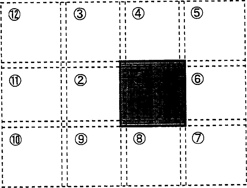
[0106] In this embodiment, after the above-mentioned reference substrate 1S is divided into a plurality of regions and photographed, the images of each region are concatenated to create and register an overall image of the reference substrate 1S. In addition, between adjacent areas, an overlap of a predetermined number of pixels is set according to an error (hereinafter referred to as "mechanical error") generated by the movement amount of the X-axis table 6 and the Y-axis table 7 . For each of these images, pattern matching processing using image information of overlapping portions is performed, and corresponding pixels are overlapped after adjusting the correspondence relationship of pixels based on the matching results to create an appropriate overall image.

[0107] image 3 An example of image superimposition processing is shown, and the order of connection is indicated by a circled number. image 3 In the example of , the image in the center is taken as the first image,...

Embodiment 2

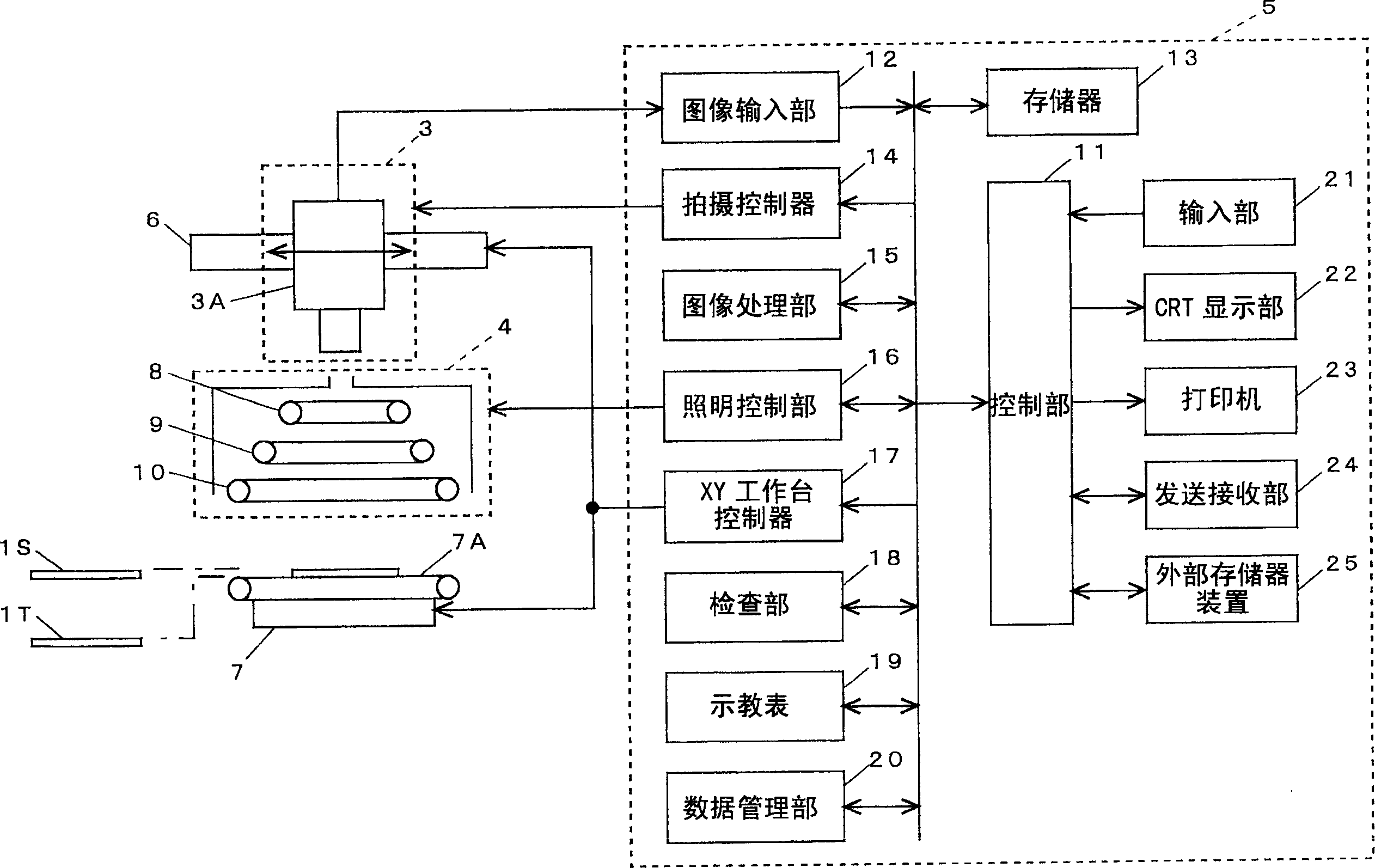
[0140] In each of the following embodiments of this second embodiment, the welding part (fillet weld) of the inspection part is taken as a premise, and the imaging target area, the setting method of the inspection area, and the relationship between the processing target image and the imaging target area are described more specifically. The detection method of deviation, etc.

[0141] According to the above figure 1 Since the colored lights from the light sources 8, 9, and 10 of the light projecting part 4 are directly projected and reflected on the surface of the fillet weld, red, green, and blue colors can be obtained corresponding to the inclination of the fillet weld. An image distributed at a prescribed scale. In the inspection of the fillet weld, by extracting these colors separately, and comparing their position and area with the judgment reference value, it is possible to judge whether the inclination state is good or not.

[0142] Figure 10 It is an image showing t...

Embodiment 3

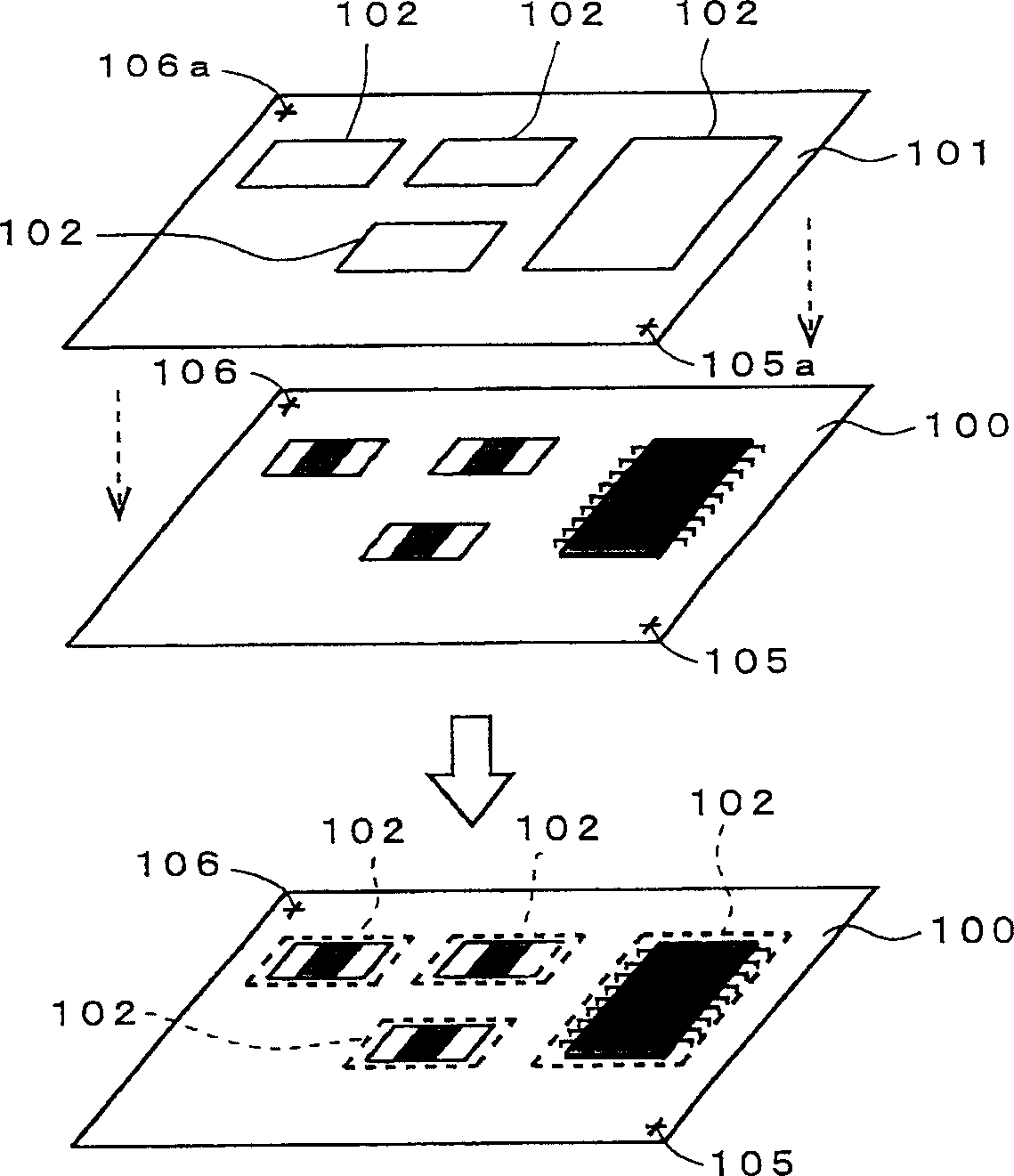
[0165] In the above-mentioned embodiment 2, it is assumed that the portion to be inspected on the substrate is included in any image constituting the overall image, but if Figure 15 As shown, there is a case where a component 56 (the component shown in the figure is a QFP) to be inspected straddles between images. In such a case, as in the first embodiment, it is preferable to set an imaging target area at an arbitrary position on the overall image 103 .

[0166] In Example 3, after the overall image 103 of the reference substrate 1S is created, the imaging target area 57 is set so that the entire part 56 is included in the image 103, the set position is registered, and the image in the imaging target area 57 is cut out. , and register as the reference image.

[0167] In addition, the setting of the imaging target area 57 can be performed using the image image of the above-mentioned board, but it is not limited thereto. can be set.

[0168] Also, there is no doubt that the...


PUM


Abstract

The invention provides a substrate checking method and a substrate checking device, completing high-precision setting of the checking area of a checked part to improve checking precision. The invention comprises the following steps: an overall image (103) of the substrate of a checking object is made in advance; correspondence is set up in advance between a checking area (31) and the checked part on the overall image (103); during checking, a camera (3A) is located at a position corresponding to a shooting object area (30) to carry out shooting; when a processing object image (40) is obtained, an area (41) corresponding to the processing object image (40) is extracted from the overall image (103); the amount of deviation (Delta x, Delta y) of the shooting object area (30) relative to the area (41) is calculated; in addition, the set location of the checking area (31) is corrected by means of the amount of deviation (Delta x, Delta y), and a checking area is set on the processing object image (40) according to the corrected coordinates.

Description

technical field [0001] The present invention relates to a method for inspecting the presence or absence of components, positional deviation, properness of soldering, etc., using an image obtained by photographing a component-mounted substrate (hereinafter sometimes simply referred to as "substrate"), and a substrate for implementing the method Check the device. Background technique [0002] The applicant has developed a substrate inspection device that automatically inspects the mounting state and soldering state of components using an image of a component-mounted substrate (see Patent Document 1). This substrate inspection apparatus includes: a substrate stage supporting a substrate to be inspected; a camera for photographing the substrate; a stage (X-axis stage, Y-axis stage) for moving the substrate stage and the camera along a horizontal plane, etc. . During inspection, the field of view of the above-mentioned camera corresponds to a predetermined area of ​​the substra...

Claims


Application Information

Patent Timeline
IPC IPC(8): G01N21/956G06K9/03
Inventor 村上清浅野靖典木下崇四谷辉久
Owner ORMON CORP
Why Eureka
Try Eureka