Supercharge Your Innovation With Domain-Expert AI Agents!

Test structure for testing leavings in semiconductor device through-hole

A technology for testing structures and semiconductors, applied in the direction of semiconductor/solid-state device testing/measurement, etc., which can solve the problem of inability to directly test metal residues

Active Publication Date: 2006-05-03
SEMICON MFG INT (SHANGHAI) CORP +1
View PDF0 Cites 6 Cited by
  • Summary
  • Abstract
  • Description
  • Claims
  • Application Information

AI Technical Summary

Problems solved by technology

[0005] In order to overcome the shortcoming that the existing semiconductor device test structure cannot directly test the metal residues existing in the through-hole region, the present invention is proposed

Method used


Image

  • Test structure for testing leavings in semiconductor device through-hole
  • Test structure for testing leavings in semiconductor device through-hole
  • Test structure for testing leavings in semiconductor device through-hole

Examples


Embodiment Construction

[0032] The test structure for testing residues in through holes in semiconductor devices according to the present invention will be described in detail below with reference to the accompanying drawings.

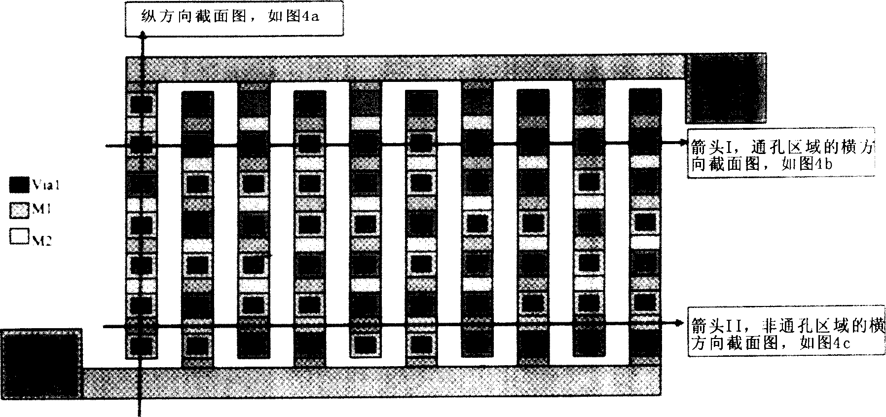
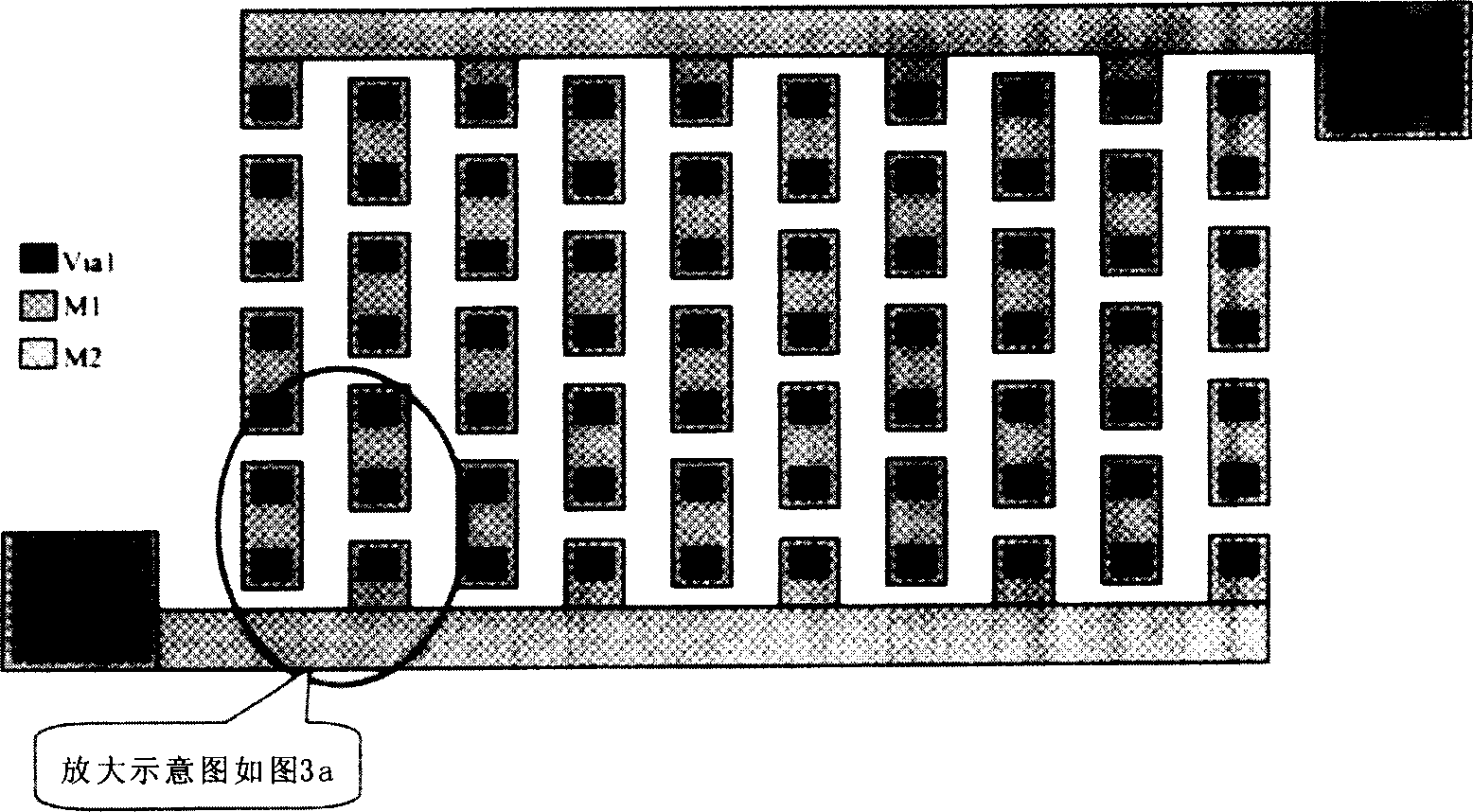
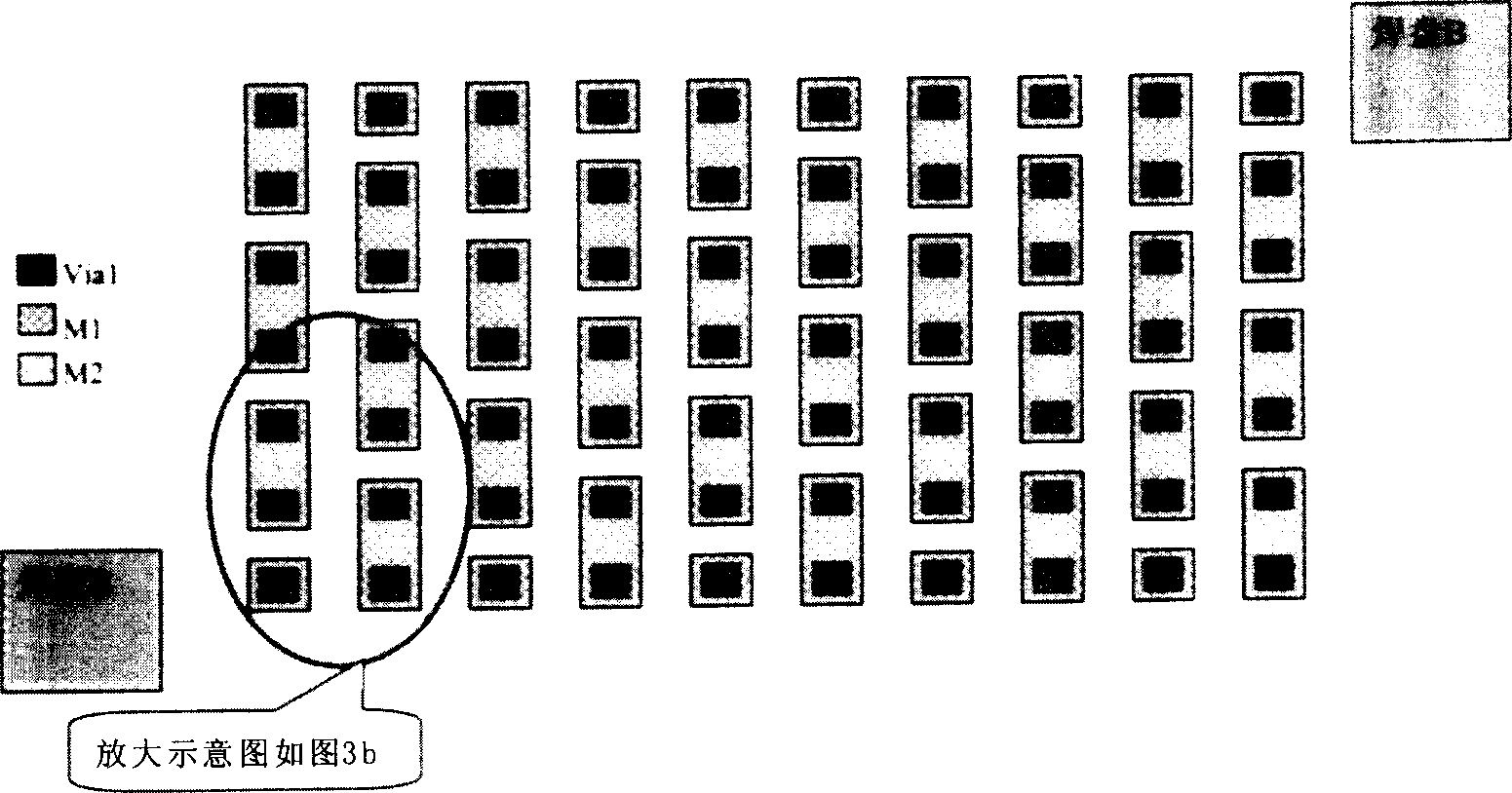
[0033] figure 1 is a top view of a pair of interdigitated comb-shaped via chain structures set in a semiconductor device, figure 1 It shows a pair of interdigitated comb-shaped via chain structures set in a semiconductor device, including: a set of comb-shaped via chain structures connected by pad A, and another set of comb-shaped via chain structures connected by pad B Chain structure, two sets of comb-shaped through-hole chain structures intersect each other to form a pair of interdigitated comb-shaped through-hole chain structures, each group of comb-shaped through-hole chain structures includes multiple through-hole chains, wherein each comb-shaped through-hole The chain structure includes the first metal layer (M1), the via layer (Vial) and the second metal layer (M2) ...


PUM


Abstract

The invention provides a structure for measuring the residuum of the semiconductor, which arranges a pair of finger V sharp comb type via hole. It comprises: a first group comb type via hole chain structure which uses welding plate A to connect and a second group comb type via hole chain structure which uses welding plate B to connect, wherein each group of comb type via hole chain structure comprises a plurality of via hole chains; two groups of comb type via hole chain structures interlocked with each other to form a pair of finger V sharp comb type via hole chain structure; each comb type via hole chain is formed by a first mental layer M1, a plurality of via hole layers Via 1 and a second mental layer M2.

Description

technical field [0001] The present invention relates to test structures in semiconductor devices, and in particular to test structures for testing residues in vias in semiconductor devices. Background technique [0002] Through the failure analysis of the burn-out failure samples and the high-temperature operating life (HTOL) test failure samples of semiconductor devices, it is found that the metal residue in the via region in the semiconductor device is one of the main failure mechanisms. [0003] In the current common semiconductor device test structure, because the adjacent metal lines interfere with the test results, there is no suitable structure to test the metal residue in the via area, and it is impossible to determine that the metal residue in the via area is reliable for semiconductor devices. sexual influence. [0004] In fact, the general semiconductor device test structure cannot evaluate the reliability of the product by determining whether there are metal res...

Claims


Application Information

Patent Timeline
Patent Type & Authority Applications(China)
IPC IPC(8): H01L21/66
Inventor 陈祯祥吴启熙
Owner SEMICON MFG INT (SHANGHAI) CORP
Features
  • R&D
  • Intellectual Property
  • Life Sciences
  • Materials
  • Tech Scout
  • Unparalleled Data Quality
  • Higher Quality Content
  • 60% Fewer Hallucinations
Learn More