
Method and device for managing transmitting buffer area in field programmable gate array

A technology for sending buffers and buffers, applied in memory address/allocation/relocation, electrical components, transmission systems, etc., to solve problems such as occupying memory blocks

Inactive Publication Date: 2006-06-07
ZTE CORP
View PDF1 Cites 11 Cited by
  • Summary
  • Abstract
  • Description
  • Claims
  • Application Information

AI Technical Summary

Problems solved by technology

However, this patent cannot solve the problem that the buffer occupies a large number of memory block (BLOCKRAM) resources inside the FPGA when the length of the frame to be processed is very long

Method used


Image

  • Method and device for managing transmitting buffer area in field programmable gate array
  • Method and device for managing transmitting buffer area in field programmable gate array
  • Method and device for managing transmitting buffer area in field programmable gate array

Examples


Embodiment Construction

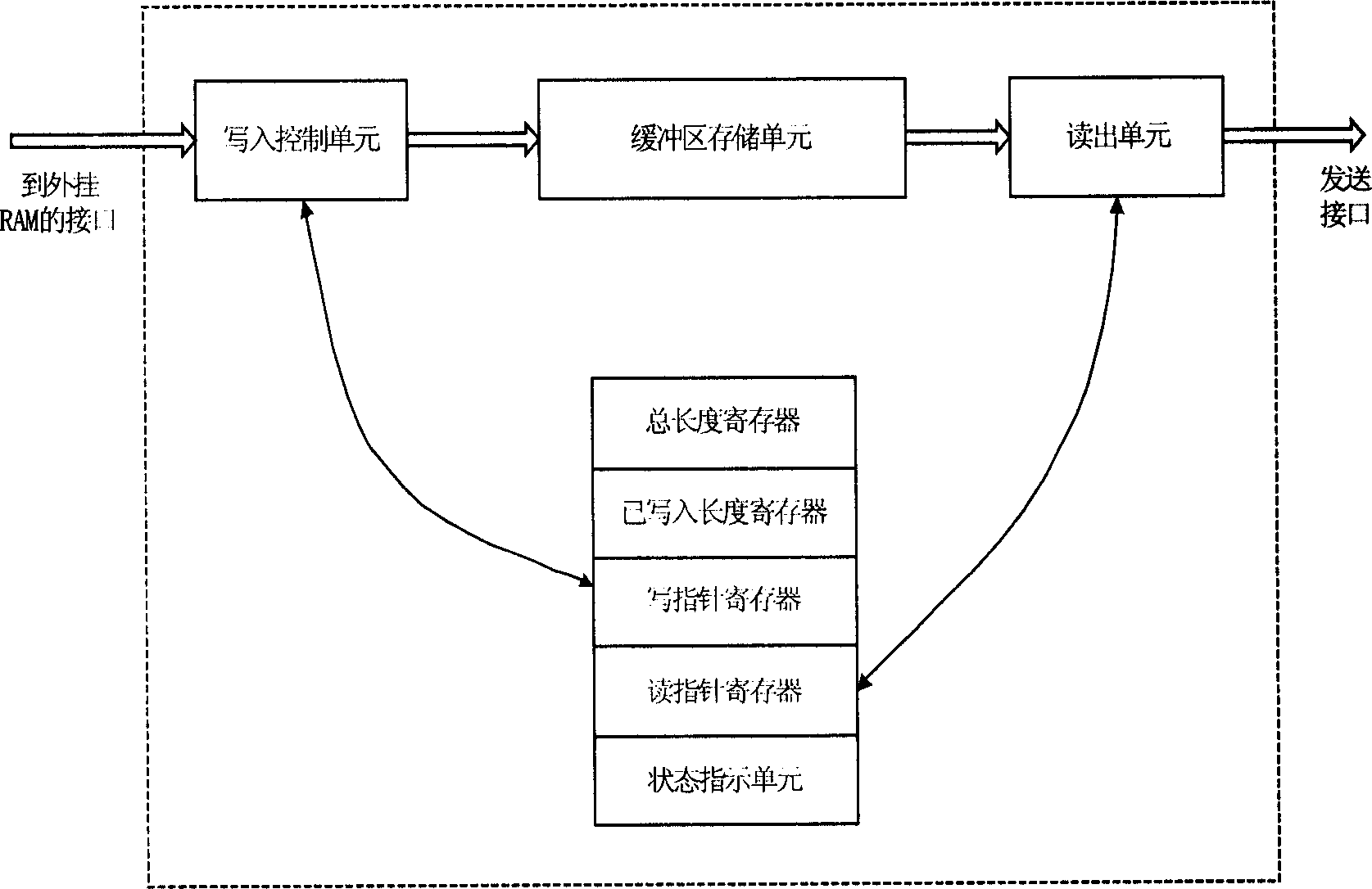
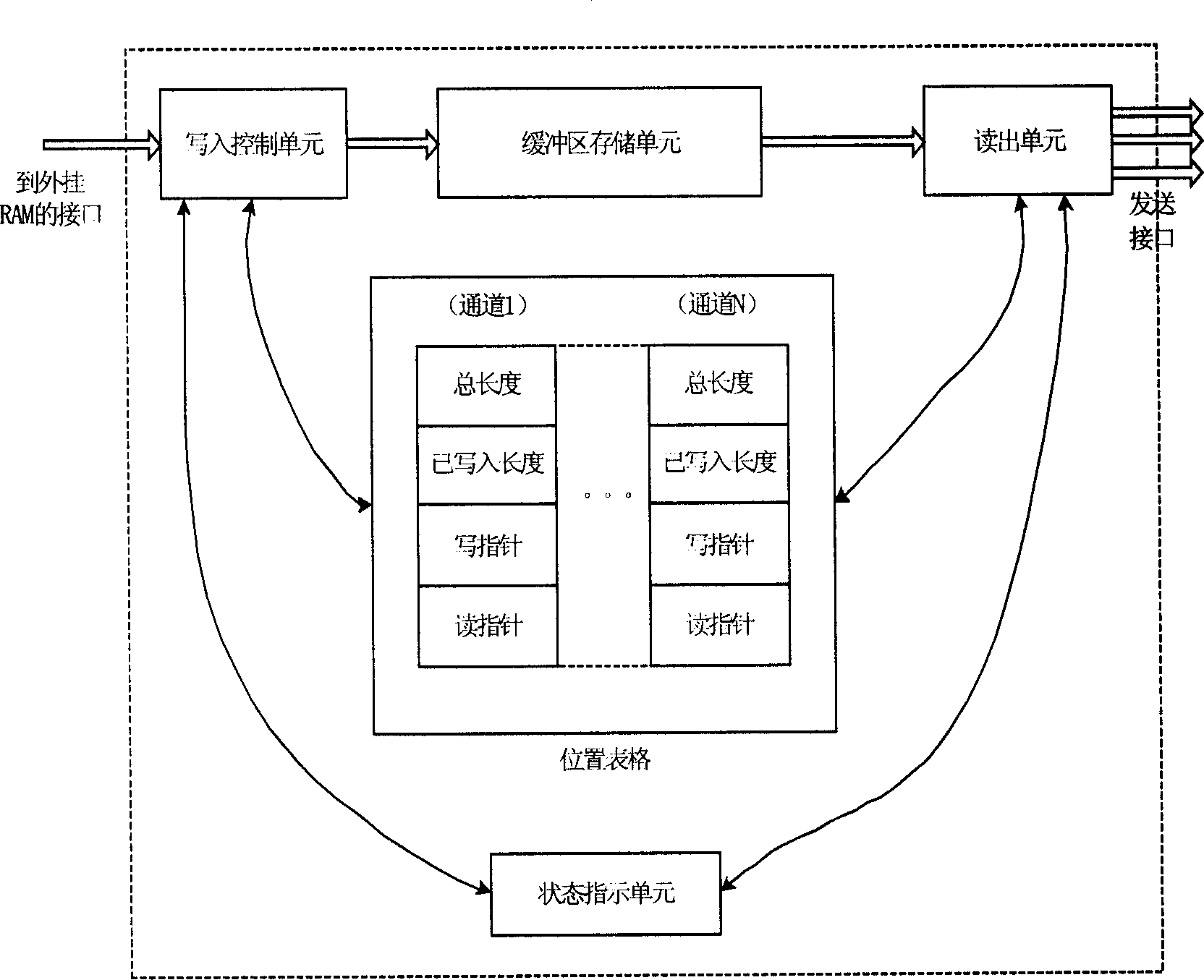
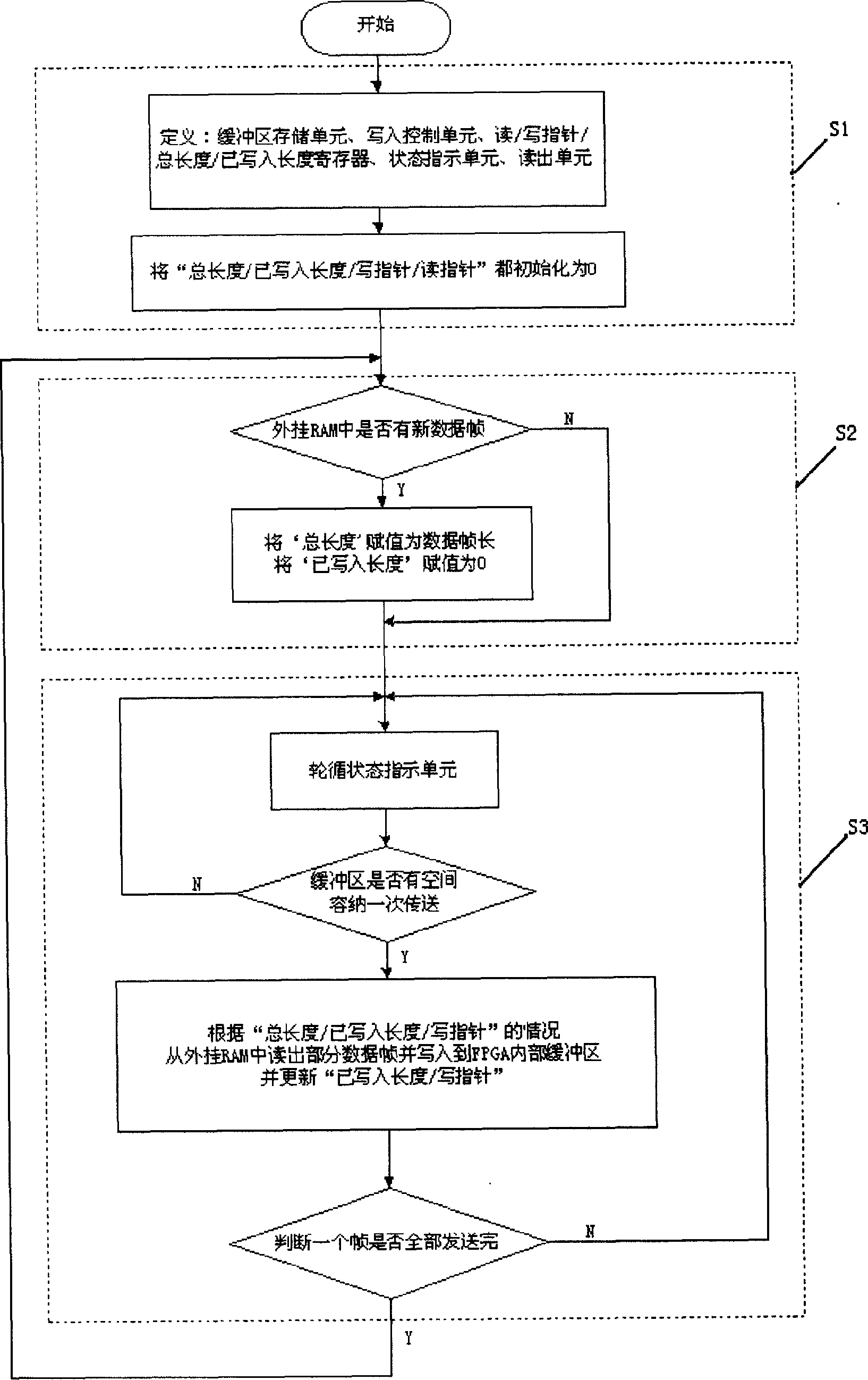
[0028] The present invention will be described in further detail below in conjunction with the accompanying drawings.

[0029] exist figure 1 Shown is the structural diagram of the present invention in the case of a single channel. When there is a data packet in the external RAM, the write control unit continuously inquires the status indicator unit, and if it is found to be '1', it means that the data that can be transmitted once can be accommodated, and then it is ready to write. The write control unit first refers to the "total length / written length register" to determine the length of a part of the data frame that needs to be transmitted at one time. The specific method is: subtract the written length register from the total length of the data frame to obtain the length of the remaining part of the frame. Before the data frame is written into the buffer, the written length register should be 0, and the length of the remaining part of the frame at this time is equal to th...


PUM


Abstract

The present invention relates to method and device for managing the transmission buffer area in FPGA. Inside the FPGA, there are defined buffer area memory unit, write-in control unit, write / read pointer register, total length / written length register, state indication unit and read out unit. The data frames to be transmitted is first read out from the plugged RAM in several times with the write-in control unit, then written to the buffer area memory unit in FPGA, and finally read out from the buffer area memory unit and sent out with the read out unit. The present invention has very small FPGA block RAM resource occupied by the buffer area even if in case of long data frame.

Description

technical field [0001] The invention relates to a field programmable gate array (FPGA), in particular to a method and a device for managing a sending buffer in the field programmable gate array (FPGA). Background technique [0002] In the current FPGA design in the communication field, it is often necessary to temporarily store the processed data frame in the external large-capacity RAM, and then move the data frame into the sending buffer inside the FPGA, and finally send it out. Usually the method is that the capacity of the sending buffer is at least one full data frame length. Whenever there is data to send and the space in the first-in-first-out buffer (FIFO) exceeds the frame length; start moving the entire packet into the FIFO. The advantage of this method is that the processing method is simple. However, when the maximum length of the processing frame type is relatively long and the number of transmission channels is relatively large, the required FPGA internal sto...

Claims


Application Information

Patent Timeline
Patent Type & Authority Applications(China)
IPC IPC(8): G06F12/02H04L49/901
Inventor 林宇平
Owner ZTE CORP
Learn More