Method for realizing reutilization in printed circuit board design

A technology for a printed circuit board and an implementation method, applied in the computer field, can solve the problems of increasing the cumbersomeness of PCB design information, and achieve the effects of improving efficiency, simple implementation, and convenient and quick operation.

Inactive Publication Date: 2006-06-07
HUAWEI TECH CO LTD
View PDF0 Cites 10 Cited by
  • Summary
  • Abstract
  • Description
  • Claims
  • Application Information

AI Technical Summary

Problems solved by technology

Therefore, in order to save the effective reuse of PCB design information, it is necessary to start the corresponding preparation design for the REUSE function in the schematic design stage, which increases the cumbersomeness of reusing PCB design information.

Method used


Image

  • Method for realizing reutilization in printed circuit board design
  • Method for realizing reutilization in printed circuit board design
  • Method for realizing reutilization in printed circuit board design

Examples


Embodiment Construction

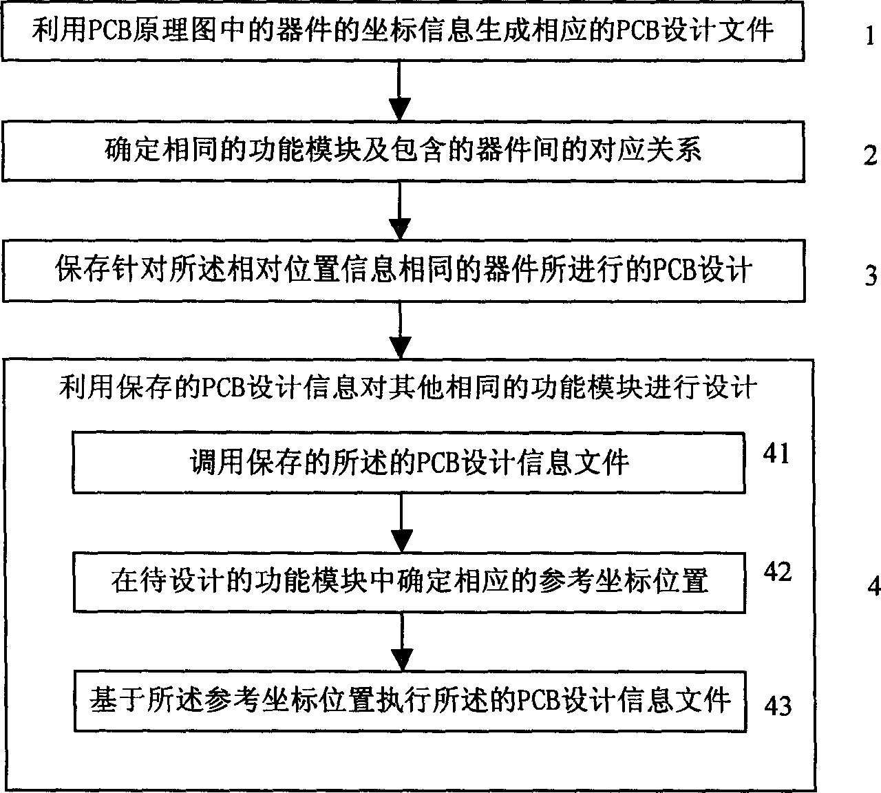
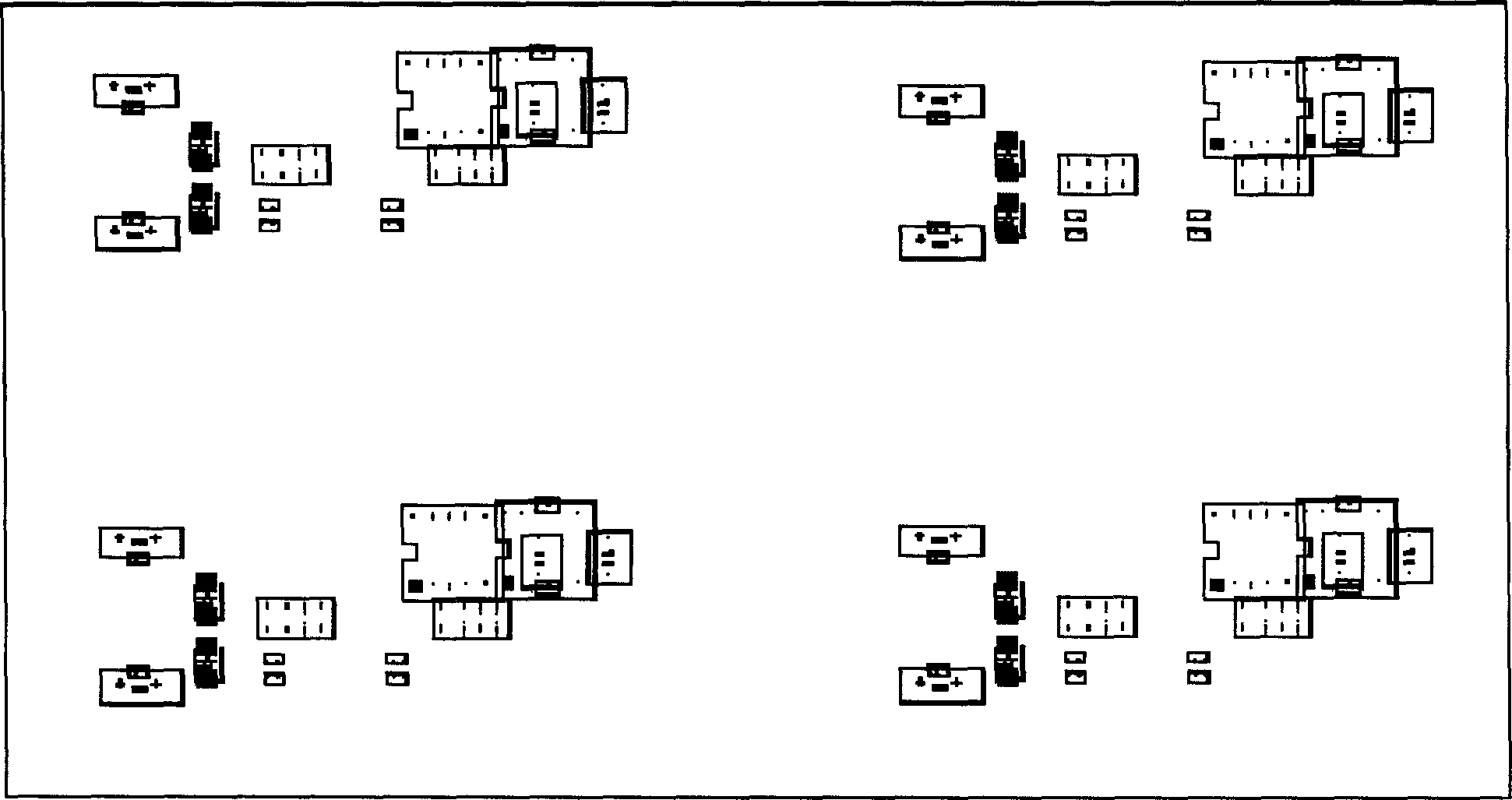
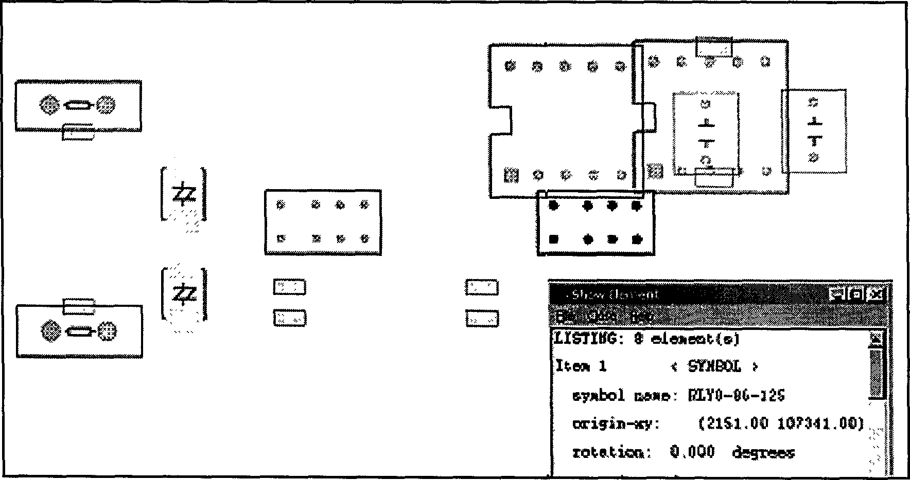
[0039] The premise of the realization of the present invention is that the relative position information between the devices contained in each identical functional module (i.e. package module) in the PCB design is the same, and on this premise, the present invention can utilize the relative position information between the same devices Information, use the saved PCB design information for one of the functional modules and the location information of other modules with the same function to carry out corresponding PCB design for the other functional modules, that is, the saved PCB design information can be effectively reused conveniently and quickly The corresponding PCB design is completed, which improves the efficiency of PCB design.

[0040] The specific implementation of the method of the present invention will be further described below with reference to the accompanying drawings. figure 1 As shown, the method of the present invention specifically includes the following ste...


PUM


Abstract

This invention relates to a PCB design reuse method. It contains determining every function module containing device and function module with same position information, making PCB design to store relative design information, when making PCB design to other same function module it can be done according to stored design information. Said invention raises PCB design efficiency. And has convenient operation.

Description

technical field [0001] The invention relates to the technical field of computers, in particular to a method for realizing reuse of PCB (printed circuit board) design. Background technique [0002] In the PCB design process, it is often the case that the same functional module is used multiple times on the same PCB. Based on this situation, in order to improve the efficiency of PCB design, PCB design engineers usually hope that when designing the same functional modules in the same PCB, only one of the functional modules should be specifically designed for the PCB, while other identical functional modules can be designed according to the PCB design. The PCB design information of the functional modules completed by the engineer automatically completes the corresponding PCB design, that is, the effective reuse of PCB design is realized. In this way, not only the consistency among the functional modules on the PCB can be ensured, but also the design efficiency of the correspond...

Claims


Application Information

Patent Timeline
Patent Type & Authority Applications(China)
IPC IPC(8): H05K3/00
Inventor 李广生
Owner HUAWEI TECH CO LTD
Why Eureka
Try Eureka