Light-emitting diode packaging structure and method for making same
A technology of light-emitting diodes and packaging structures, applied in electrical components, electrical solid-state devices, circuits, etc., can solve the problems of SMD LED luminous efficiency and poor quality, abnormal SMD LEDs, and difficulty in making reflective grooves, etc., so as to be suitable for mass production , good heat dissipation, and simplified manufacturing process
- Summary
- Abstract
- Description
- Claims
- Application Information
AI Technical Summary
Problems solved by technology
Method used
Image

Examples
Embodiment Construction
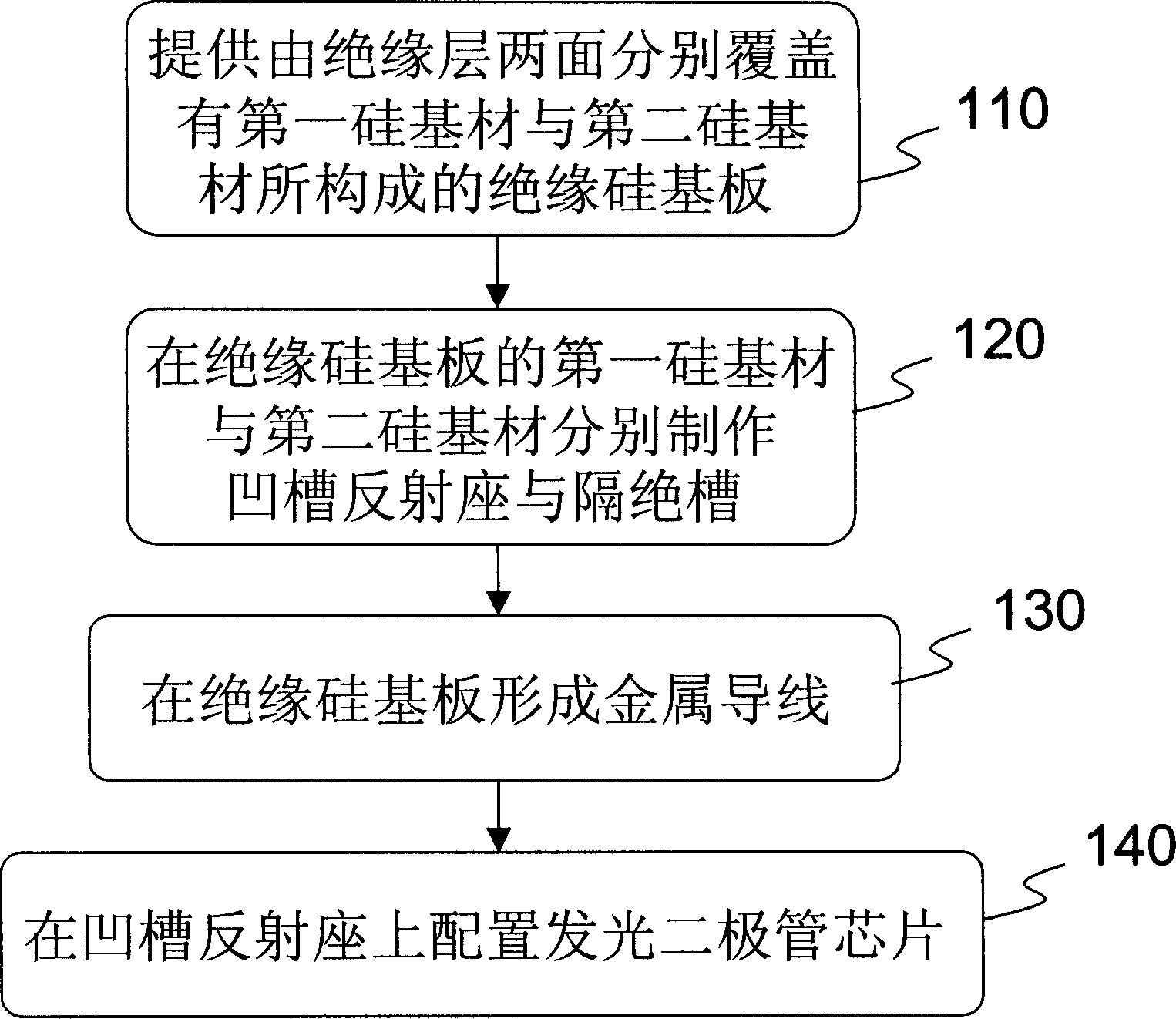
[0047] The schematic flow chart of the first embodiment of the present invention is as follows figure 2 As shown, the steps include:
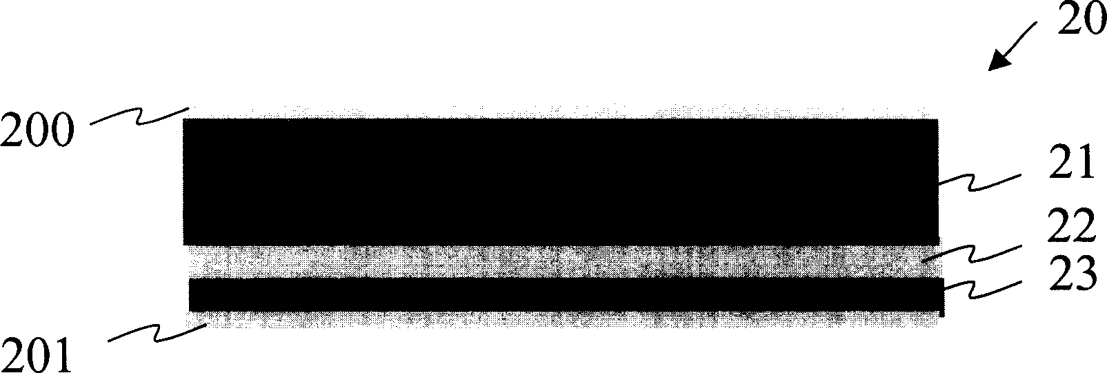
[0048] First, provide an insulating silicon substrate composed of a first silicon substrate and a second silicon substrate on both sides of the insulating layer (step 110);
[0049] Then, fabricate groove reflection seats and isolation grooves on the first silicon base material and the second silicon base material of the insulating silicon substrate respectively (step 120);
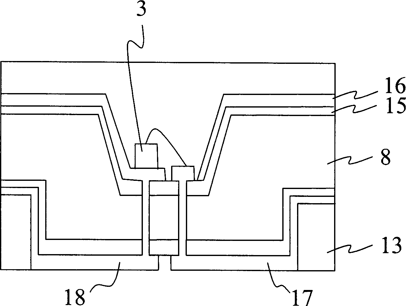
[0050] forming metal wires on a silicon-on-insulator (SOI) substrate (step 130), for electrical connection between the light-emitting diode chip and the first silicon substrate and the second silicon substrate of the silicon-on-insulator substrate;
[0051] Arrange light-emitting diode chips on the groove reflective seat (step 140), and electrically connect to the positive and negative electrodes externally connected to the insulating silicon substrate respectively throu...
PUM
 Abstract
Description
Claims
Application Information
 - R&D Engineer
- R&D Manager
- IP Professional
- Industry Leading Data Capabilities
- Powerful AI technology
- Patent DNA Extraction
Browse by: Latest US Patents, China's latest patents, Technical Efficacy Thesaurus, Application Domain, Technology Topic.
© 2024 PatSnap. All rights reserved.Legal|Privacy policy|Modern Slavery Act Transparency Statement|Sitemap