Scan test design method, scan test circuit, scan test circuit insertion cad program, large-scale integrated circuit, and mobile digital device

A technology of scanning test and design method, which is applied in the direction of detecting faulty computer hardware, circuits, calculations, etc., can solve problems such as increased power consumption, increased circuit area, and increased number of delay elements, and achieves improved pass rate and good design guarantee Effect

Inactive Publication Date: 2006-07-19
PANASONIC CORP
View PDF1 Cites 12 Cited by
  • Summary
  • Abstract
  • Description
  • Claims
  • Application Information

AI Technical Summary

Problems solved by technology

Therefore, there are problems of an increase in circuit area, an increase in power consumption, and an increase in leakage current when many delay elements are in standby.
[0008] As above figure 2 As in the example shown, in the conventional circuit that interconnects FF circuits between different clock trees, if a circuit that is easily affected by interference such as crosstalk (crosstalk) and voltage drop (IR drop) is used In the design of semiconductor micro-processes, the delay time of the clock tree part is affected by the above-mentioned interference and voltage drop, and more margin is required when transmitting shift data, so the delay element inserted in the scan shift circuit part further increase in the number of
The further increase in the number of delay elements caused by the above-mentioned test simplification design will further increase the circuit area of ​​the large-scale integrated circuit, and even lead to an increase in power consumption and a significant increase in the leakage current of many delay elements in standby

Method used


Image

  • Scan test design method, scan test circuit, scan test circuit insertion cad program, large-scale integrated circuit, and mobile digital device
  • Scan test design method, scan test circuit, scan test circuit insertion cad program, large-scale integrated circuit, and mobile digital device
  • Scan test design method, scan test circuit, scan test circuit insertion cad program, large-scale integrated circuit, and mobile digital device

Examples


no. 1 example

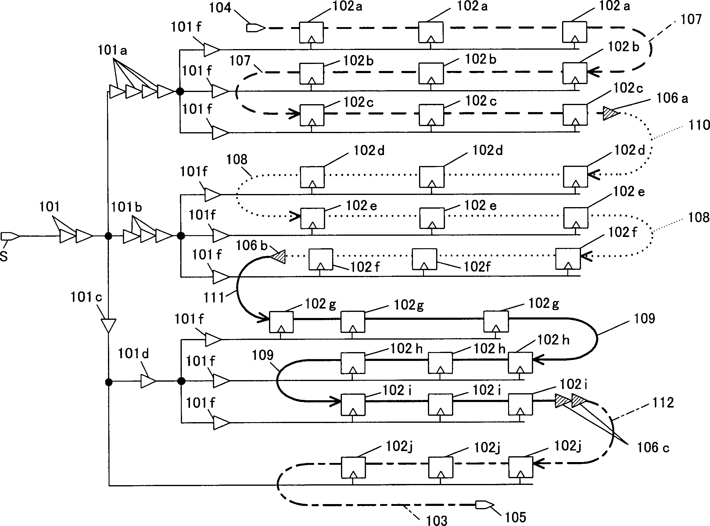
[0054] figure 1 It shows the structure of the scan shift register of the scan shift circuit realized by the test simplification design method in the first embodiment of the present invention, and especially shows the structure of the CTS buffer and the connection relation of the scan shift register. Below, use the figure 1 Be explained.

[0055] exist figure 1 Among them, 101 is a clock delay adjustment buffer, 101a to 101f are CTS buffers, and a clock tree T is formed. The clock tree T is divided into buffers 101a, 10b and 101c, each branch is further divided into three buffers 101f. A clock signal is supplied to the clock terminals of the FF circuits 102a to 102j which are many flip-flop circuits (hereinafter referred to as FF circuits) through this clock tree T.

[0056] In the design method of this embodiment, firstly, a scanning shift register is formed by taking a plurality of FF circuits driven by the last-stage element 101f of the CTS as the minimum unit. So, u...

no. 2 example

[0060] Next, a second embodiment of the present invention will be described.

[0061] In the representation of the first embodiment figure 1 In this case, three FF circuits 102a are used to constitute a sub-scanning chain, and three FF circuits 102b, 102c, 102d, 102e, 102f, 102g, 102h, 102i, and 102j are used in the same manner as the three FF circuits 102a. Each scanning shift register is constituted. Therefore, in the first embodiment, the scan test circuit can be constituted by connecting the respective input and output of the shift register to the scan input or the scan output of the LSI. However, in this case, in a large-scale circuit, the following situation will be caused, that is, the number of test terminals is huge, and due to the increase of test cost and the constraints of external terminals of large-scale integrated circuits, the terminals are not enough, and it is difficult to realize the test. Simplistic design.

[0062] Therefore, by connecting the sub-scan...

no. 3 example

[0066] Next, a third embodiment of the present invention will be described.

[0067] The third embodiment shows a design method adopted when the number of scan test terminals (scan input terminals and scan output terminals) cannot exceed the restricted number of terminals in the second embodiment.

[0068] If the restriction on the number of scan test terminals cannot be met in the second embodiment, or if the number of scan chains needs to be further reduced for other reasons, it is necessary to interconnect scan shift registers with different stages of CTS buffers. In this case, firstly, as in the second embodiment, the shift registers having the same number of CTS buffer stages are preferentially connected in series through the sub-scan chain inter-connecting networks 107 , 108 and 109 .

[0069] Next, at figure 1 Among them, as the second priority order of connection, the shift registers with the smallest relative buffer stage difference from the clock supply point S to ...


PUM


Abstract

In designing a scan test circuit, in the final stage element (101f) unit of a clock tree (T), a plurality of flip-flop circuits (102a to 102a, 102b to 102b, 102c to 102c, ...) driven by the final stage element (101f) are connected in series, thereby constituting a sub-scan chain. Moreover, sub-scan chains having a minimum relative stage difference (i.e., one stage difference) of the number of delay elements from the clock supply point (S) of the clock tree (T) are connected to one another. Furthermore, the sub-scan chains are connected to one another in such a manner that data is shifted from a flip-flop circuit having a large clock delay to a flip-flop circuit having a small clock delay. Accordingly, the number of delay elements inserted into the data line of the shift register as the hold time guarantee in the shift operation of the scan shift register is reduced, thereby reducing the power consumption.

Description

technical field [0001] The present invention relates to a large-scale integrated circuit design method, a large-scale integrated circuit test circuit, and a large-scale integrated circuit design computer-aided design program. The design assurance and control of the hold time of operation is a test simplification design technique that accompanies the increase of circuit area, the increase of power consumption and the increase of leakage current with the insertion of hold guarantee delay elements. Background technique [0002] With regard to test simplification design, the case of scan test design is by far the most general. according to Figure 5 Describe the scan test design. [0003] exist Figure 5 Among them, after designing the register transfer level (RTL), the register transfer level file 501 is used as input data to carry out logic synthesis computer-aided design program 502 to generate a gate level netlist (netlist) 503 . First, by using the scan test circuit inser...

Claims


Application Information

Patent Timeline
Patent Type & Authority Applications(China)
IPC IPC(8): G01R31/28G01R31/317G01R31/3185G06F11/22G06F17/50H01L21/822H01L27/04
CPCG01R31/318594G01R31/318591G01R31/318575
Inventor 宝积雅浩
Owner PANASONIC CORP
Why Eureka
Try Eureka