

Micro contact-element and making method
A manufacturing method and micro-contact technology, which can be used in contact manufacturing, contact components, semiconductor/solid-state device manufacturing, etc., and can solve problems such as bending of silicon substrates, increased failure rate, and poor process qualification rate.
- Summary
- Abstract
- Description
- Claims
- Application Information
AI Technical Summary
Problems solved by technology
Method used
Image

Examples
Embodiment Construction
[0024] In order to enable a further understanding and recognition of the features and objectives of the present invention, the following preferred embodiments are enumerated and described below with accompanying drawings.
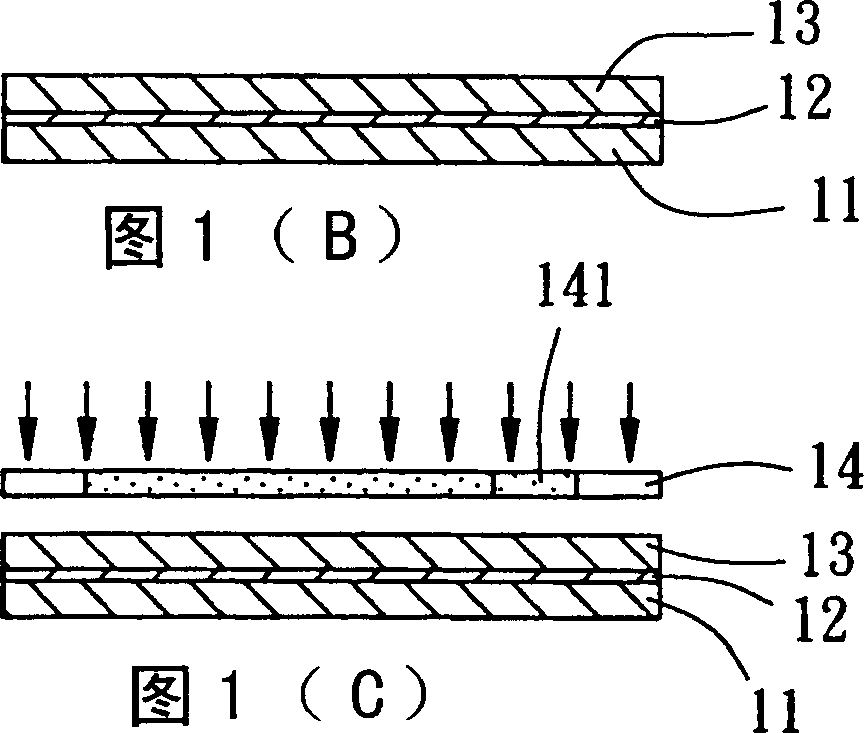
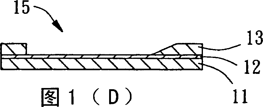
[0025] Please refer to Fig. 1 (A) to Fig. 1 (H), which is a manufacturing method of a micro-contact element provided by the first preferred embodiment of the present invention, wherein the micro-contact element manufactured by the following manufacturing method is an example of a probe , whose steps include:
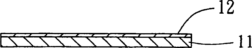
[0026] a) As shown in FIG. 1(A): Laying and forming a conductive film 12 on a substrate 11 with a non-conductive surface.
[0027] Wherein, the material of the substrate 11 can be a semiconductor material, a metal plate coated with a non-conductive material, a polymer material, a ceramic material, a composite material, etc., such as a silicon substrate. The conductive film 12 can be a metal with good adhesion, such as titanium metal; the conductive f...
PUM
 Abstract
Description
Claims
Application Information