Semiconductor device and manufacturing method thereof

a semiconductor and semiconductor technology, applied in the field of semiconductor devices, can solve the problems of insufficient aperture ratio, conventional problem, beam blur, etc., and achieve the effects of reducing the aperture ratio of the mask, high dimension accuracy, and improved resolution

Inactive Publication Date: 2005-11-15
HITACHI LTD
View PDF5 Cites 59 Cited by
  • Summary
  • Abstract
  • Description
  • Claims
  • Application Information

AI Technical Summary

Benefits of technology

[0014]On the other hand, the method contrived by the present inventor (disclosed in JP-A No. 153351 / 2001) divides a mask into a plurality of masks so that the pattern density (aperture ratio) becomes approximately equal in each subfield or within each influential range of the Coulomb interaction. This is because the current value changes, thereby the beam blur caused by the Coulomb interaction comes to differ among masks if the aperture ratio differs among fields. Therefore, the complementary mask division is done so that the aperture ratio becomes approximately the same among the divided masks and the beam blur is prevented from generating an extreme difference among the masks.
[0022]Under such circumstances, it is an object of the present invention to provide a method for manufacturing semiconductor devices, which can form patterns at high accuracy and a high throughput with use of electron beam projection equipment that uses complementary masks.
[0025]Such complementary mask division can reduce the aperture ratio of the mask that includes fine patterns or patterns requiring high dimension accuracy, thereby the resolution is improved. In addition, because fine patterns and patterns requiring high dimension accuracy are gathered in the first mask region, the second mask region comes to include comparatively large patterns, that is, rough patterns that are not requiring such high dimension accuracy as that of the first mask region. Generally, the aperture ratio becomes high in the second mask region, but there is no need to lower the irradiation current there to improve the printing accuracy, since the region includes only rough patterns. The current value can thus be decided in accordance with the first mask region having low aperture ratios, thereby the throughput is lowered.
[0026]Next, a description will be made for a method for improving the throughput according to the present invention more in detail with reference to FIG. 19. In the upper half of FIG. 19 is shown a relationship between an irradiation current to masks and pattern dimension errors when the mask aperture ratio is changed. In the lower half of FIG. 19 is shown a relationship between the irradiation current to masks and the throughput. Pattern dimension errors are caused by various factors such as a mask dimension, non-uniformity of the current among subfields, etc. Generally, however, the error becomes larger in proportion to an increase of the beam blur on wafer. As a result, the larger the aperture ratio or irradiation current increases, the larger the mask transmission current becomes, and the larger the mask transmission current becomes, the more the beam blur increases. Consequently, the pattern dimension error becomes large. On the other hand, the exposure time is in proportion to the required dose / irradiation current to masks, so that the throughput increases together with the irradiation current to masks. Here, the dimension accuracy required for fine patterns is defined as Afine and the accuracy required for rough patterns is defined as Arough. If a mask is divided complementarily so that two complementary masks become equal in aperture ratio D2, fine patterns are usually put into both of the two complementary masks. In order to suppress the exposure error of each mask at Afine or less, therefore, the current becomes I1, thereby the throughput becomes TP1. On the other hand, the present invention premises that a mask is divided complementarily so that only one of the two masks includes fine patterns and the aperture ratio of the mask is defined as D1 and the aperture ratio of the other is defined as D3. (In this connection, it is also assumed that the aperture ratio of the mask that includes fine patterns is smaller than that of the other mask. This assumption will be satisfied in most cases as to be described in the embodiments of the present invention. The exceptions will also be described in those embodiments.) To suppress each dimension error within a predetermined allowable value, the current becomes I2, thereby the throughput becomes TP2. The present invention can thus improve the throughput.

Problems solved by technology

If the aperture ratio of layout data is high, however, the aperture ratio is not reduced enough even by such complementary mask division.
This has been a conventional problem.
Although the aperture ratio becomes a half of the previous one, the aperture ratio is still large, thereby the Coulomb interaction causes a beam blur to occur.
And, as shown in FIG. 4C, a pattern resolution defect results.
This has also been another conventional problem.
However, the value of the irradiation current to masks cannot be changed in each subfield.
Therefore, if any one of the several thousands of subfields on a chip has an aperture ratio of 20% or more, such as those 601 shown in FIG. 6B-1 and FIG. 6B-2, and it includes any pattern requiring high dimension accuracy, the current must be lowered for the printing, thereby the throughput comes to be limited.

Method used


Image

  • Semiconductor device and manufacturing method thereof
  • Semiconductor device and manufacturing method thereof
  • Semiconductor device and manufacturing method thereof

Examples


first embodiment

(First Embodiment)

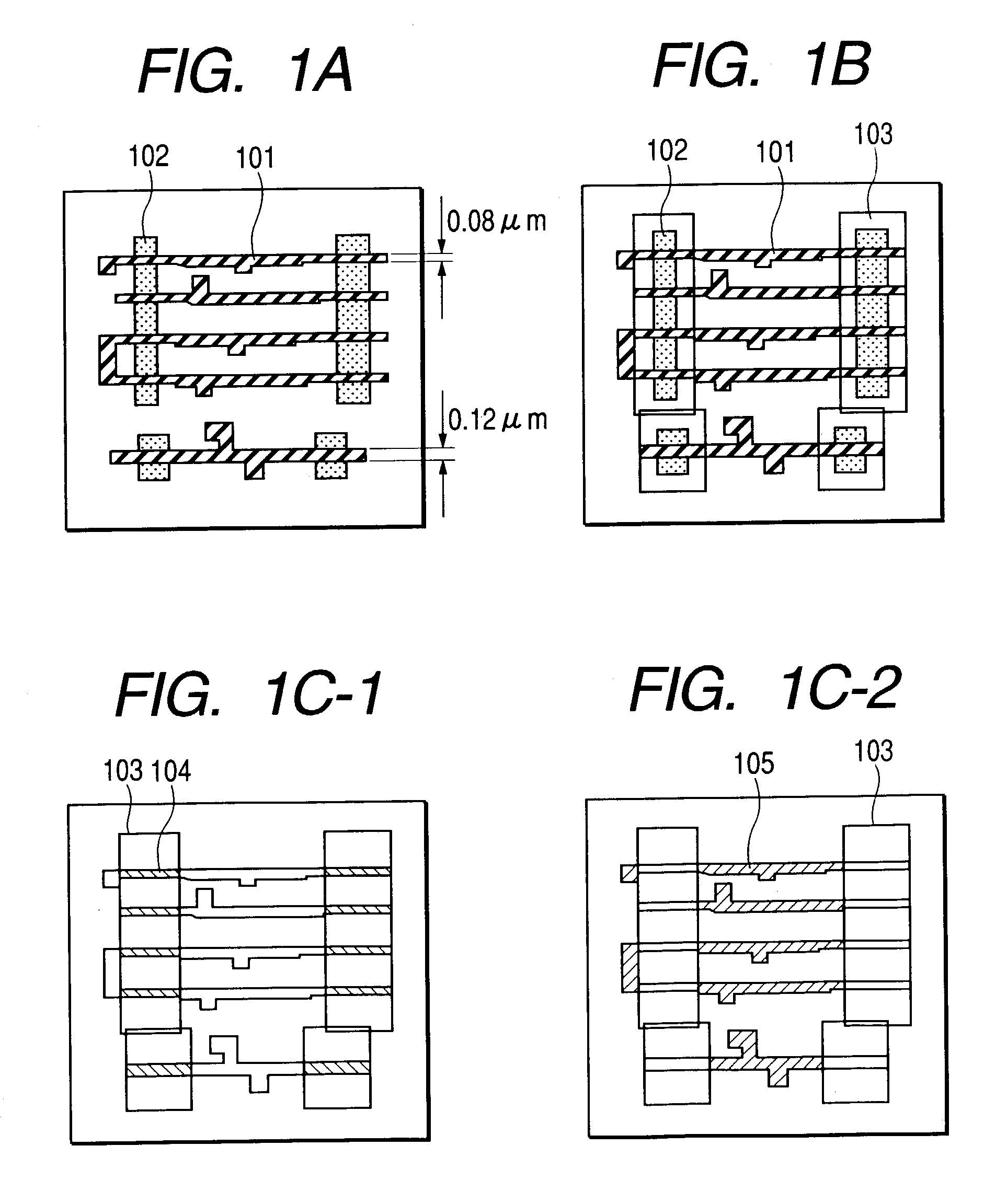
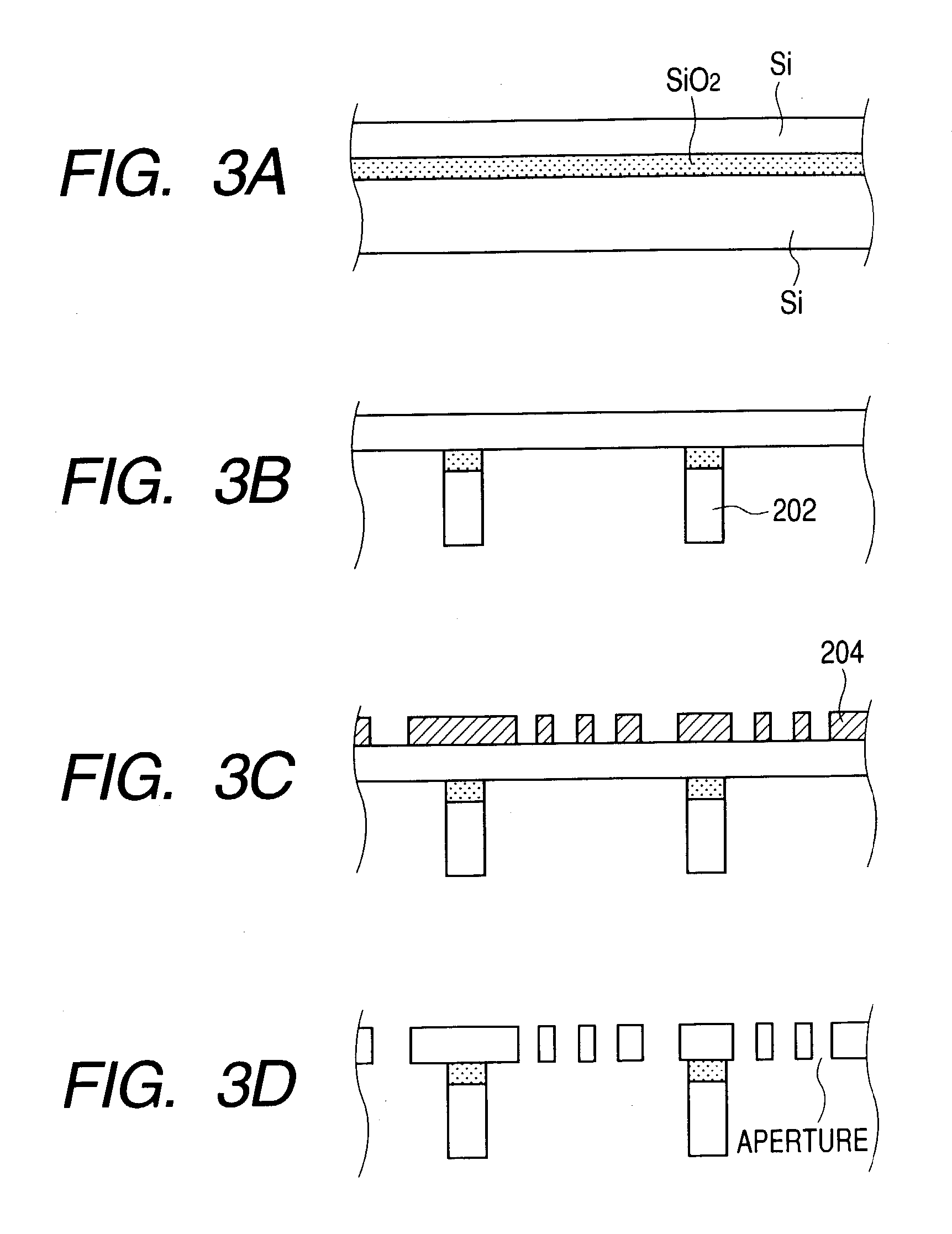
[0051]Hereunder, the preferred embodiments of the present invention will be described with reference to the accompanying drawings. At first, a description will be made for the first embodiment, which is a method for dividing a mask complementarily to form some of the gate layer patterns with reference to FIGS. 1A, 1B, 1C-1 and 1C-2. The selected patterns that require specially high dimension accuracy are formed on an active layer.

[0052]FIGS. 1A, 1B, 1C-1 and 1C-2 show mask data of active regions 102 of a MOSLSI and gate patterns 101 formed on the active regions. In FIGS. 1A, 1B, 1C-1 and 1C-2, the gate patterns 101 on the active regions 102 are 0.08 μm and 0.12 μm in width. In a range up to at least at a portion separated by 0.15 μm from the active region, each gate pattern is laid out at the same width of the gate pattern on the active region 102 in consideration of the total errors of both gate layer and active region. In other regions, the gate patterns are laid...

second embodiment

(Second Embodiment)

[0058]This second embodiment describes a method for dividing a mask into complementary masks in consideration of the required accuracy of the gate patterns.

[0059]FIG. 7A shows gate patterns 701 and active region patterns 702. Each gate pattern 701 is drawn at the minimum pattern width of 0.1 μm and at the minimum pattern space of 0.16 μm. If both thick and thin gates co-exist, almost all the gates are located on active regions, and the mask is divided just like in the first embodiment, then the aperture of the mask that includes the patterns on the active regions becomes higher than those of other masks. To avoid this, the mask is divided into two complementary masks so that the aperture ratio of the mask that includes shorter gate patterns of those located on the active regions becomes lower. In other words, patterns having a width of a predetermined value or less and the edges of aperture patterns adjacent to those patterns at predetermined spaces or less are ex...

third embodiment

(Third Embodiment)

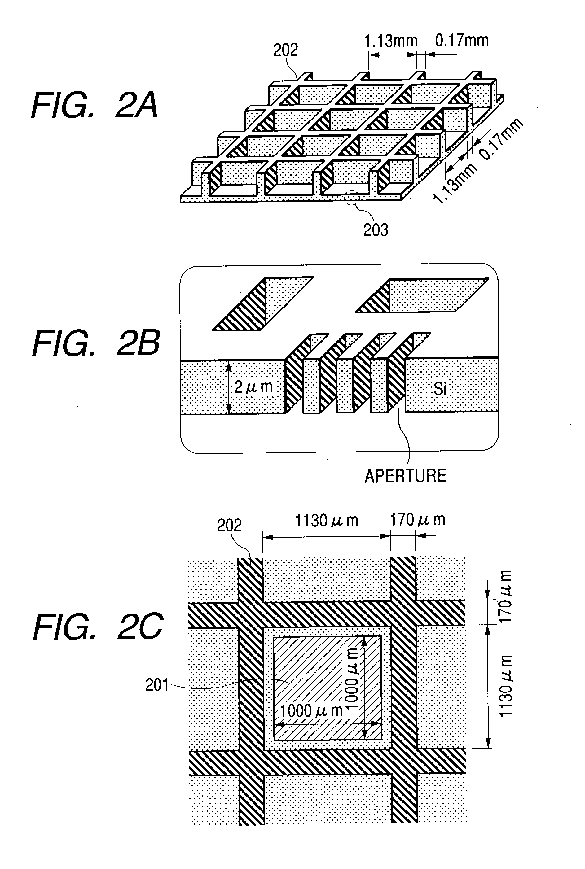
[0065]Next, a description will be made for the complementary mask division to be made when subfields are in the influential range of the Coulomb interaction with reference to the flowchart shown in FIG. 14. The patterns in the object layer are laid out at the minimum width of 0.8 μm and at the minimum spaces of 0.08 μm. In this connection, the aperture ratio of each subfield must be under 20% so as to meet the utilization condition of the electron beam projection equipment to realize the accuracy of 10 nm or less for patterns of not more than 0.1 μm width to be irradiated by the electron beam and not to be irradiated by the electron beam (hereinafter, to be referred to as fine patterns).

[0066]On a chip constituted by 6×6 subfields, the aperture ratio of each subfield is decided as shown in FIG. 16A. In FIGS. 16A, 16B-1, 16B-2, 16C-1, and 16C-2, each subfield whose aperture ratio value is encircled has an aperture ratio that exceeds 20%. On the other hand, each shad...


PUM

PropertyMeasurementUnit
thicknessaaaaaaaaaa
thicknessaaaaaaaaaa
thicknessaaaaaaaaaa

Abstract

A method is provided for solving a problem that the fine processing property is degraded by an increase of a current applied to complementarily divided masks in an electron beam projection process. In the method, the complementarily divided masks used for electron projection are used whereby one mask is used for patterns requiring high dimensional accuracy and another is used for other patterns. Consequently, it is possible to lower the current applied to the patterns requiring high dimensional accuracy to realize high printing accuracy. In addition, the highly accurate patterns can be formed at a high throughput.

Description

BACKGROUND OF THE INVENTION[0001](1) Field of the Invention[0002]The present invention relates to a method for manufacturing semiconductor devices used for semiconductor integrated circuits, liquid crystal panels, etc. More particularly, the present invention relates to a method for manufacturing semiconductor devices with use of an electron beam projection method that is a lithographic technique employed for forming fine patterns of the semiconductor devices, as well as a method for forming the masks used by the method and a method for generating data for the masks.[0003](2) Description of the Related Art[0004]Lithographic techniques are usually employed for forming patterns of semiconductor integrated circuits, etc. And, a light, an electron beam, or the like is used as the energy beam. The photo-lithography among those lithographic techniques has been improved in resolution by changing the wavelength of the light source from a g-line (436 nm) to such short wavelengths as an i-lin...

Claims


Application Information

Patent Timeline
Patent Type & Authority Patents(United States)
IPC IPC(8): G03F1/16G03F1/20G03F1/68G03F7/20H01L21/027
CPCG03F1/20Y10S430/143H01J2237/31794H01L21/027
Inventor MONIWA, AKEMIYAMAMOTO, JIROMURAI, FUMIOFUKUDA, HIROSHI
Owner HITACHI LTD
Why Eureka
Try Eureka